WO2017015554
Processors suitable for the execution of a computer program include, by way of example, both general and special purpose microprocessors, and any one or more processors of any kind of digital computer.
【0114】
コンピュータプログラムの実行に適したプロセッサは、一例として、一般及び専用マイクロプロセッサの両方、及びあらゆる種類のデジタルコンピュータの一以上のプロセッサを含む。
Generally, a processor will receive instructions and data from a read-only storage area or a random access storage area or both.
一般に、プロセッサは、読み出し専用記憶領域又はランダムアクセス記憶領域又はその両方から指示及びデータを受け取る。
Elements of a computer include one or more processors for executing instructions and one or more storage area devices for storing instructions and data.
コンピュータの要素は、指示を実行するための一以上のプロセッサと、指示及びデータを保存するための一以上の記憶領域デバイスを含む。
Generally, a computer will also include, or be operatively coupled to receive data from, or transfer data to, or both, one or more machine-readable storage media, such as mass PCBs for storing data, e.g., magnetic, magneto-optical disks, or optical disks.
一般に、コンピュータは、磁気、磁気光学ディスク、又は光学ディスクのようなデータ保存用の集合基板といった一以上の機械可読保存媒体も含む又はそれらとデータの受信、送信、又はその両方を行えるように動作可能に結合されている。
US2021068268(JP)
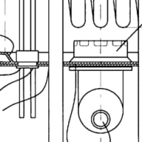
[0087] The multilayer substrate 101 according to the present preferred embodiment is manufactured, for example, through the following steps.
【0067】
本実施形態に係る多層基板101は、例えば次の工程で製造される。
FIG. 7 is a sectional view sequentially showing a manufacturing process of the multilayer substrate 101 .
図7は、多層基板101の製造工程を順に示す断面図である。
In FIG. 7, for convenience of explanation, the manufacturing process on one chip (individual piece) is described, but the actual manufacturing process of the multilayer substrate is performed in the state of a collective board.
なお、図7では、説明の都合上ワンチップ(個片)での製造工程で説明するが、実際の多層基板の製造工程は集合基板状態で行われる。
*assembly board