US10666084
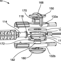
[0067] If(*論理yes/no;whenは時間、タイミング)the electronic device detects(*現在形だが意味は過去)the presence of a surface while in the non-scanning mode (block 1200 ) or while in the first scanning mode (block 1202 ),
【0059】
電子装置が、非スキャニングモード(ブロック1200)又は第1のスキャニングモード(ブロック1202)中に表面の存在を検出した場合、
the method continues at block 1204 where the electronic device determines if the surface is a charging surface of a charging device.
方法はブロック1204に進み、電子装置は、この表面が充電装置の充電面であるかどうかを判定する。
Any one of the techniques described earlier can be used to determine whether the surface is a charging surface.
表面が充電面であるかどうかは、上述した技術のいずれか1つを用いて判定することができる。
For example, the charging surface can include one or more triggering elements such as colored and/or differently shaped structural elements, a pattern, or conductive contacts that may be imaged or detected electrically by the electronic device.
例えば、充電面は、電子装置が撮像又は電気的に検出できる色付きの、及び/又は異なる形状の構造要素、パターン、又は導電性接点などの1又は2以上のトリガ要素を含むことができる。
In another example, the charging device may include a light pipe that propagates(*他動詞)light from an emitter in the electronic device to a detector in the electronic device.
別の例では、充電装置が、電子装置内の発光体から電子装置内の検出器に光を伝搬する光導波管を含むことができる。
US8428404
SUMMARY
【0006】
概要
[0008] One embodiment of the present disclosure provides a hybrid integrated module.
本開示の一実施形態は、ハイブリッド集積モジュールを提供する。
This hybrid integrated module may include a semiconductor die mechanically coupled face-to-face by an adhesive to an integrated device in which the substrate has been removed.
このハイブリッド集積モジュールは、基板が取除かれた集積デバイスに対して、接着剤により、対向して機械結合される半導体ダイを含み得る。
For example, the integrated circuit may include an optical waveguide
たとえば、集積回路は光信号を伝搬する光導波管を含むことができ、
that conveys an optical signal, which is fabricated on a silicon-on-insulator (SOI) wafer in which the back side silicon substrate or handler has been completely removed(*完了形).
これは裏面側のシリコン基板またはハンドラが完全に除去されたシリコンオンインシュレータ(SOI)ウェハ上に製造される。
Moreover, an optical device may be disposed on the bottom surface of an oxide layer (such as the buried-oxide or BOX layer) in the integrated device,
さらに、光学デバイスを集積デバイスの酸化物層(たとえば埋込酸化物またはBOX層)の底面に配置することができ、
and the thickness of the semiconductor layer (such as silicon) and the thickness of the oxide layer in the integrated device
集積デバイスの半導体層(たとえばシリコン)の厚さおよび酸化物層の厚さは、
may be defined so that the optical signal is evanescently coupled between the optical waveguide and the optical device.
光信号が光導波管と光学デバイスとの間でエバネセントに結合されるよう、固定され得る。
US10969604
[0010] In one aspect, an apparatus for a three-dimensional display comprises
【0011】
一側面において、3次元ディスプレイのための装置は、
a waveguide having a pair of opposed faces configured to propagate(*他動詞)radiation along a length of the waveguide between the faces;
面間で導波管の長さに沿って放射を伝搬するように構成された一対の対向面を有する導波管と、
a radiation source optically coupled to the waveguide and configured to transmit the radiation to the waveguide;
導波管に光学的に結合され、放射を導波管に伝送(*「送信」だと変;信号ではない)するように構成された放射源と、
at least one prismatic element having a face optically coupled to at least one of the faces of the waveguide, the face of the prismatic element having a perimeter;
導波管の面のうちの少なくとも1つに光学的に結合された面を有する少なくとも1つのプリズム要素であって、プリズム要素の面は、周辺を有する少なくとも1つのプリズム要素と、
and a layer of image modulating material optically coupled to an area of at least one of the faces of the waveguide, at least a portion of the area being located outside the perimeter of the face of the prismatic element.
導波管の面のうちの少なくとも1つのエリアに光学的に結合された画像変調材料の層であって、エリアの少なくとも一部は、プリズム要素の面の周辺外に位置する、画像変調材料の層とを備えている。
////////
[0034] Light rays as shown propagating(*自動詞)in waveguide 202
【0035】
導波管202内を伝搬する示されるような光線は、
remain trapped by total internal reflection
when the refractive index of the medium external to the waveguide is less than the refractive index of the material from which the waveguide is made,
導波管の外部の媒体の屈折率が導波管が作製される材料の屈折率未満であるとき、
全内部反射によって捕獲されたままであり、
and the angle of incidence of the light with respect to the normal to the planar surface of the waveguide is greater than the critical angle, θC =sin− (n1 /n2 ),
導波管の平面表面の法線に対する光の入射角は、臨界角、θC=sin-1(n1/n2)を上回り、
where n1 and n2 are the refractive indices of the medium external to the waveguide and the medium of the waveguide itself, respectively.
n1およびn2は、それぞれ、導波管の外部の媒体および導波管自体の媒体の屈折率である。
///////////
[0090] FIG. 6 shows an arrangement(*配置;複数要素)by which three different staggered waveguides, each provided with a different fluorescent material, might be coupled together to form a composite, full color image.
【0083】
図6は、3つの異なる交互導波管による配置を示し、3つの異なる交互導波管の異なる蛍光性材料を具備し、各々は、一緒に結合され、複合フルカラー画像を形成し得る。
Waveguide 606 , in which light of one wavelength propagates, is optically coupled to waveguide 604 by a dichroic material 610
1つの波長の光が伝搬する導波管606は、ダイクロイック材料610によって、導波管604に光学的に結合され、
located between opposing faces of the waveguides 604 , 606 in an end region of the lower waveguide 606 .
ダイクロイック材料610は、下側導波管606の端部領域において導波管604、606の対向面間に位置している。
US10886617
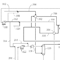
[0077] Signal traces 82 may convey radio-frequency signals to and from feed probe 85 .
【0077】
信号トレース82は、高周波信号を給電プローブ85との間で伝達することができる。
Feed probe 85 may electromagnetically couple the radio-frequency signals on signal traces 82 into dielectric resonating element 92 .
給電プローブ85は、信号トレース82上の高周波信号を誘電体共振要素92に電磁的に結合することができる。
This may serve to excite one or more electromagnetic modes (e.g., radio-frequency cavity or waveguide modes) of dielectric resonating element 92 .
これは、誘電体共振要素92の1つ以上の電磁モード(例えば、高周波空洞モード又は導波路モード)を励起するよう機能し得る。
When excited by feed probe 85 , the electromagnetic modes of dielectric resonating element 92
給電プローブ85によって励起されると、誘電体共振要素92の電磁モードは、
may configure the dielectric resonating element to serve as a waveguide that propagates the wavefronts of radio-frequency signals 104 along the length of dielectric resonating element 92 (e.g., in the direction of the Z-axis of FIG. 6), through top surface 98 , and through display 14 .
誘電体共振要素92の長さに沿って(例えば、図6のZ軸の方向に)、上面98を介して、そしてディスプレイ14を介して、高周波信号104の波面を伝搬する導波路として機能するように誘電体共振要素を構成することができる。
US2016109733
[0009] The polarization of the modulation electrodes with the modulation voltage
【0005】
変調電圧による変調電極の分極は、
allows, by electro-optic effect in the substrate, to vary the optical refractive index of the waveguide in which the guided lightwave propagates, as a function of this modulation voltage.
基板内の電気光学効果により、導波光波が伝搬する導波路の光屈折率をこの変調電圧の関数として変化させることを可能にする。
US8768112
[0029] In the illustrated embodiment, a fiber cladding 118 is circumferentially disposed about the fiber core 112 and,
【0025】
図示の実施形態では、ファイバクラッド118は、ファイバコア112の周りに円周方向に配置され、
in one embodiment, has an outer diameter of approximately 125 microns and is made from pure silica.
一実施形態では、約125ミクロンの外径を有し、純粋シリカから作られる。
In one embodiment, the fiber cladding 118 is configured to act as a waveguide for light propagation through the fiber core 112 .
一実施形態では、ファイバクラッド118は、ファイバコア112を通って光を伝搬する導波路として作用するように構成される。
The broadband tunable light source 110 is positioned in light communication with the optical fiber cable and emits a near infrared light that propagates through the fiber core 112 .
広帯域の調整可能な光源110は、光ファイバケーブルと光通信するように位置決めされ、ファイバコア112を通って伝搬する近赤外光を放出する。
US9786266
SUMMARY
概要
[0006] The inventors have recognized and appreciated that it would be advantageous,
本発明者らは、
within the context of an acoustic treatment system,
音響加工システムの環境においては、
to direct acoustic energy into a space defined by a waveguide chamber, which appropriately channels the acoustic energy so as to create a focal zone of acoustic energy.
音響エネルギーの焦点ゾーンを生成するように音響エネルギーを適切に伝搬する導波路チャンバによって定義された空間内に音響エネルギーを導くこと
が有利であることを認識及び理解した。