


US11051736(MEDTRONIC XOMED INC [US])
[0106] Referring again to FIGS. 2-4, the cuff portion 160 extends distally directly from the distal portion 158 of elongate body 152 . In one embodiment, the cuff portion 160 includes a first finger 172 and second finger 174 arranged in a side-by-side relationship ( FIGS. 2-5) and extending from a base portion 177 .

US10293131(FISHER & PAYKEL HEALTHCARE LTD [NZ])
[0072] FIG. 44 is a front view of the endoskeleton and the exoskeleton of the mask assembly of FIG. 37, with the endoskeleton and the exoskeleton positioned side by side for comparison.

US11801544(GED INTEGRATED SOLUTIONS INC [US])
[0023] FIG. 11 is a perspective view of a punching station having side by side stamping units that are actuated by a controller based on the type of material of the strip material passing through the stamping unit;
////////
[0053] The punching station 104 accepts the stock S from a properly positioned coil at the stock supply station and performs a series of stamping operations on the stock as the stock S passes through the punching station. The punching station 104 comprises a supporting framework 238 ( FIG. 11 ) fixed to the factory floor. A stock driving system 140 moves the stock through the station until the stock is grasped by a downstream drive system 145 ( FIG. 11 ) described in more detail in the Calcei et al. '681 Patent. Stamping units 144 , 146 , 148 , 150 , 152 , 154 spaced along the station 104 in the direction of stock movement perform individual stamping operations on the stock S.

US8106520(MICRON TECHNOLOGY INC [US])
[0025] FIG. 3 shows a partial cross-section of an IC package 300 having devices 310 and 320 and an interposer 330 , according to various embodiments of the invention. IC package 300 may also include a base 390 having conductive elements 399 to transfer information to and from IC package 300 . IC package 300 may use a structure that includes interposer 330 and structure portions 341 , 342 , and 343 to transfer signals between base 390 and or both of devices 310 and 320 . As shown in FIG. 3, base 390 , devices 310 and 320 , and interposer 330 are arranged in a stack in the z-dimension and attached to each other by conductive joints 301 (e.g., solder, copper, or other materials). IC package 300 may include an enclosure 302 and an interior 303 , which may be filled with insulation material such as epoxy-based molding compound. The components of IC package 300 , such as devices 310 and 320 , interposer 330 , and structure portions 341 , 342 , and 343 , may be enclosed inside enclosure 302 .
[0027] Device 310 may include functions and material similar to or identical to device 110 of FIG. 1 or device 210 of and FIG. 2. As shown in FIG. 3, device 310 may include multiple dice such as dice 311 and 312 located side by side with each of other in the x-dimension and on the same stack level in the z-dimension, which is perpendicular to x-dimension. Each of dice 311 and 312 may include conductive contacts 313 and 314 located at opposite surfaces of the die and vias 315 extending through the die and coupled to conductive contacts 313 and 314 . Each of dice 311 and 312 may also include conductive paths 316 going through the die. Conductive paths 316 may include conductive material 317 inside vias 315 . Each of dice 311 and 312 may also include additional conductive paths (not shown in FIG. 3) to transfer signals between base 390 and device 320 . The additional conductive paths may not go through vias that extend through the die. Device 310 may include a memory device where each of dice 311 and 312 may include other components, such as memory cells and related circuitry, which are omitted from FIG. 3 to help focus on the embodiments described herein.

US9814377(WELCH ALLYN INC [US])
[0040] Referring to FIGS. 8(a )-8(c ) , various versions of supported LEDs and LED supporting members are shown in various combinations for enabling a specific (e.g., white) light to be spectrally produced for the described illumination system. For purposes of describing these embodiments, similar parts are labeled with the same reference numerals for the sake of clarity. An LED supporting member 820 defined by a ring-like configuration supports a plurality of LEDs in a spaced circumferential manner about a defined center opening 821 for positioning and aligning same in relation to a light guide, such as those previously discussed in FIGS. 5(a )-7(d ) . The LEDs are attached either using adhesives or other suitable means in regard to a facing surface 823 of the supporting member 820 onto a single or independently mounted circuit boards. In a first version shown in FIG. 8(a ) , a plurality of LEDs are disposed in a spaced circumferential configuration provided on the facing surface 823 of the supporting member 820 .
//////
[0041] Referring to FIG. 8(b ) , there is provided an alternative configuration of plural LEDs as positioned at each of the spaced circumferential positions 824 of the supporting ring 820 . More specifically and according to this version, a pair of amber LEDs 830 are disposed at the first circumferential position 824 and positioned in side by side relation. A second pair of green LEDs 834 are disposed at the second circumferential position 824 , also in side by side relation with a third pair of blue LEDs 838 being disposed, according to this example, at the third circumferential position 824 . As in the preceding version, this pattern of side by side LEDs is repeated over the remaining five (5) circumferential positions 824 , as depicted. It should be noted that though two LEDs are shown herein in side by side relation at each ring position, it will be readily understood that the number of LEDs provided at each circumferential position of the supporting element can easily be varied, for example, depending on the application required.

US8322079(YKK CORP AMERICA [US])
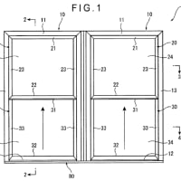
[0037] As shown in FIG. 1, the single-hung window 1 comprises a so-called “dual-type” single-hung window, which is installed in an opening in the exterior wall of a building, such as a house, for separating an interior space and an exterior space of the building. The dual-type single-hung window 1 has two window frames 10 disposed side by side or in horizontal juxtaposition with an upper sash 20 and a lower sash 30 supported within each of the window frames 10 . The window frames 10 each include a head member 11 , a sill member 12 and a pair of side or jamb members 13 , 13 connected together into a rectangular shape. The upper and lower sashes 20 and 30 each have a sash frame including a top rail 21 , 31 , a bottom rail 22 , 32 , and a pair of side rails or stiles 23 , 33 connected together into a rectangular shape, and a panel of glazing (double-glazing) 24 , 34 held within the sash frame.

US8029014(GRACO CHILDRENS PROD INC [US])
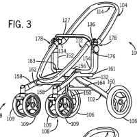
[0033] Turning now to the drawings, an exemplary stroller is generally depicted at 100 in FIGS. 1-4 and is constructed in accordance with the teachings of the present disclosure. In this example, the stroller 100 generally has a frame assembly 102 , a seat assembly 104 ( FIG. 1) supported by the frame assembly 102 , and a plurality of wheels supporting the frame assembly 102 on a ground surface. The frame assembly 102 in the disclosed example includes a pair of rear wheels 106 and a pair of front wheel assemblies indicated generally at 108 . In this example, each front wheel assembly 108 has two wheels 109 spaced apart side by side. The configuration and construction of the front wheel assemblies 108 and the rear wheels 106 can vary considerably and yet fall within the spirit and scope of the present invention.

US5491302(TESSERA INC [US])
One aspect of the present invention provides a method of connecting a part of a semiconductor chip or other microelectronic assembly having a plurality of contacts disposed in a row to a connection component including a plurality of leads having connection sections disposed side by side in said row. The method comprises the steps of juxtaposing the connection component with the part of the semiconductor chip assembly and connecting the connection section to the corresponding contacts. In the step of juxtaposing the row of connection sections is disposed above the row of contacts in alignment therewith, so that each connection section is offset from a corresponding contact in a first direction along said rows. In the connecting step, the connection sections and the corresponding contacts are connected by performing a connection cycle on the connection sections in sequence along the row in the first direction. Each connection cycle for each connection section includes the step of engaging one or more connections section with a tool and moving the engaged section or sections and the tool downwardly and in a second direction opposite to said first direction into engagement with the corresponding contacts, whereby during each connection cycle the tool and the engaged connection section or sections move away from the next adjacent unconnected connection section. Because the tool moves away from the next unconnected connection section, there is increased clearance for the tool shank.

//////
In a method according to one embodiment of the invention, the semiconductor chip is initially disposed on a substrate or a flat support surface 25. Then, the connection component 20 is positioned atop the chip 12 (see FIG. 1) with the bottom layer 24 of the connection component facing the top surface 14 of the chip. The connection component is juxtaposed with the chip in such a manner that the gap 26 of the connection component is aligned with the row of contacts 18 of the chip. Thus, a longitudinal axis of the gap 26, coincides with or extends substantially parallel to the lengthwise axis of the row of contacts or connection pads 18. The connection section of each lead is positioned across the gap 26 extending transversely to the lengthwise axis of the row of contacts. The juxtaposing step may be performed using conventional positioning elements of the type commonly employed for positioning semiconductor chips with respect to TAB (tape automated bonding) tape. The positioning equipment includes one or more video cameras 108, computer equipment 110 and servomechanisms 112. During the juxtaposing step, the video camera and computer equipment detect the positions of the fiducial marks 102 and 104 on the connection component body and chip, and may also command the servomechanism to adjust the relative positions of the connection component and chip accordingly so as to bring the connection component and chip to the desired alignment. Even with such corrections, however, it is not normally possible to bring all portions of the connection component body into perfect alignment with the associated parts of the chip.


※コメント投稿者のブログIDはブログ作成者のみに通知されます