US2009238734(特表2011-515854)
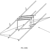
"2. The substrate support of claim 1, wherein the roll-formed indents are arranged in a grid pattern(格子状パターン)."
WO2015199682(特表2017-520786)
"5. The integrated circuit of claim 1, wherein the cells are formed on a grid of(格子状の)diffusion lines and gate lines."
US2014346357(特表2015-513067)
"11. The photoconductive device of claim 1, wherein the one or more plasmonic contact electrodes are configured according to at least one shape selected from the list consisting of: a grating(格子状), a rectangular-shape(矩形), a cross-shape(十字形), a C-shape(C字形), a H-shape(H字形), a split-ring-resonator, a circular hole, or a rectangular hole(長方形穴)."
WO2013006243(特表2014-523128)
"2. A method according to Claim 1 further comprising:
forming a first gridded(格子状)metal layer on the second subcell; and
forming a second gridded metal layer on the silicon subcell,
wherein bonding the second subceil to the silicon subcell comprises establishing(設ける)metal- to-metal bonds between the first and second gridded metal layers of the second subcell and the silicon subcell."
WO2009097371(特表2011-511310)
"11. The polarization preserving front projection screen of claim 2, wherein the plurality of reflective microstructures(微細構造)are distributed in a substantially regular lattice(規則的な格子状)."
WO2007061788(特表2009-516357)
"22. The LED light unit of Claim 21 , wherein: the LED light sources are arranged on the tile in a staggered grid(ジグザグ状の格子状)extending in a direction away from the connected edge connector."
WO2016014983(特表2017-526119)
"3. The method of Claim 1, wherein the enhancement layer is at least one set of gratings(格子)formed of wavelength-sized or sub-wavelength-sized features that are arranged periodically, quasi-periodically(準周期的), or randomly."
WO2015123043(特表2017-510064)
"8. The method as claimed in claim 1 wherein the step of growing(成長させる)the layer of epitaxial rare earth oxide on the silicon substrate includes epitaxially growing(エピタキシャルに堆積)a first rare earth oxide layer substantially lattice matched to(格子が一致した)the silicon substrate and epitaxially growing a second rare earth oxide layer with a different lattice constant on the first rare earth oxide layer so that the second rare earth oxide layer is stressed."
WO2014110017(特表2016-508235)
"13. The optical phased array of claim 9, further comprising: a grating(格子), in optical communication with the at least one variable optical delay line, to diffract at least part of the corresponding portion of the coherent optical beam so as to form the far- field radiation pattern."
WO2013081793(特表2015-503235)
"1. An apparatus comprising:
a substrate having a planar(平坦な)top surface(上部表面);
a sequence of crystalline semiconductor layers being located on the planar surface and having a two-dimensional quantum well therein;
a first set of electrodes being located over the sequence, bordering(境界を接して)opposite sides of a lateral region thereof, and being controllable to vary a width of a non-depleted portion of the quantum well along the top surface;
a second set of electrodes being located over the sequence, bordering first and second channels between the lateral region and first and second adjacent lateral areas of the sequence, and being controllable to vary widths of non-depleted segments of the quantum well; and
wherein the electrodes are located such that straight lines connecting the first and second lateral areas via the channels either pass between one of the electrodes and the substrate or are misaligned to an effective [1 1 0] lattice(格子)direction of the sequence."
最新の画像[もっと見る]
-
 Are they exceptions?
3日前
-
 Are they exceptions?
3日前
-
 今年もスイカ!
3週間前
-
 今年もスイカ!
3週間前
-
 方向:冠詞
3週間前
-
 方向:冠詞
3週間前
-
 side by side
1ヶ月前
-
 side by side
1ヶ月前
-
 side by side
1ヶ月前
-
 side by side
1ヶ月前


※コメント投稿者のブログIDはブログ作成者のみに通知されます