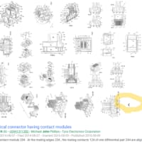
US20140007940
(Abstract)
"Disclosed are thermoplastic resin formulations for use as a light transmitting layer (e.g., encapsulant layer(封止材層)) in a photovoltaic module comprising: (a) a light transmitting thermoplastic resin, (b) at least one down conversion material that exhibits a maximum in incident radiation absorption in the range of 280 to 500 nm and a maximum in radiation emission at a relatively longer wavelength in the range of 400 to 900 nm and improves the efficiency of photovoltaic electric current generation in a photovoltaic module; and (c) a light stabilizer additive that transmits at least about 40 percent of the ultraviolet (UV) electromagnetic radiation having a wavelength in the range of from about 280 nm to about 380 nm. Also disclosed are sheet materials prepared from such resins and photovoltaic modules incorporating such sheet materials."
"7. A photovoltaic module for the conversion of incident electromagnetic radiation into electric energy, comprising: (i) a light transmitting exterior surface cover sheet; (ii) at least one light transmitting encapsulation(封止)sheet material according to claim 6 providing protection to a photovoltaic cell from environmental effects, (iii) a protective exterior surface back sheet and (iv) least one photovoltaic cell adapted to convert into electric energy electromagnetic radiation that has passed through the cover sheet and encapsulation film."
"[0084] As can be seen in FIG. 3, a PV module 10 comprises at least one photovoltaic cell 11 (in this case having a light-reactive or effective surface directed or facing upward in the direction of the top of the page) surrounded or encapsulated(封止)by light transmitting protective encapsulating component 12 (shown here as a combination of two "sandwiching" sub-layers 12a and 12b). The light transmitting cover sheet 13 has an interior surface in adhering contact with(接着接触)a front facial surface of the encapsulating film layer 12a, which layer 12a is, in turn, disposed over and in adhering contact with PV cell 11."
US7432133(特表2009-513030)
(Abstract)
"Structure and method are provided for plastic encapsulated(樹脂封止)semiconductor devices having a buffer layer of low dielectric constant and/or low loss tangent(正接)material separating the die surface from the plastic encapsulation(封止樹脂). Semiconductor wafers with substantially completed SC die are coated with the buffer layer. The buffer layer is patterned to expose the die bonding pads but leave the buffer layer over some or all of the other die metallization(チップ金属配線(?)). The die are then separated, mounted on a lead-frame or other support, wire bonded or otherwise coupled to external leads, and encapsulated(封止). The plastic encapsulation surrounds the die and the buffer layer, providing a solid structure. The buffer layer reduces the parasitic capacitance, cross-talk and loss between metallization regions on the die. An optional sealing layer may also be provided at the wafer stage between the buffer layer and the plastic encapsulation to mitigate any buffer layer porosity."
US7347352(特表2007-512714)
"Ball bonding is a common technique for interconnecting the bond pads on a semiconductor die with the contact points on a lead frame or other substrate on which the die is mounted. Electrical interconnect wires typically are run(延びる、延在、引き回す)from the bond pads on the top of the die to lead fingers on a lead frame in order to electrically connect the circuitry on the die to the pins of the lead frame that will extend from the package after the die has been encapsulated(樹脂封止). The wire bonds between the bond pads of the die and the lead fingers commonly are formed using a ball bonding machine."
US20130112942(特表2015-504459)
(Abstract)
"Composites having semiconductor structures embedded in a matrix are described. In an example, a composite includes a matrix material. A plurality of semiconductor structures is embedded in the matrix material. Each semiconductor structure includes an anisotropic nanocrystalline core composed of a first semiconductor material and having an aspect ratio between, but not including, 1.0 and 2.0. Each semiconductor structure also includes a nanocrystalline shell composed of a second, different, semiconductor material at least partially surrounding the anisotropic nanocrystalline core. An insulator layer encapsulates(封止)each nanocrystalline shell and anisotropic nanocrystalline core pairing."
US20130256741(特表2014-506263)
"40. A light emitting diode comprising: a substrate; and an encapsulant(封止材)at least partially surrounding(囲繞)the substrate and comprising a reaction product of a composition comprising; (A) an organopolysiloxane component comprising at least one of a disiloxane, a trisiloxane, and a tetrasiloxane, and having at least one of an alkyl group and an aryl group and having an average of at least two alkenyl groups per molecule, and (B) an organohydrogensiloxane component having at least one of an alkyl group and an aryl group and having an average of at least two silicon-bonded hydrogen atoms per molecule, in the presence of (C) a catalytic amount of a hydrosilylation catalyst component; with the proviso that(但し)the encapsulant has a refractive index ranging from 1.40 to 1.60 at 632.8 nm wavelength."
最新の画像[もっと見る]
-
 バズリクソンズA2:第16週
2日前
-
 DAZN(ダゾーン):メール配信停止ボタンくらい付けとけ
1週間前
-
 DAZN(ダゾーン):メール配信停止ボタンくらい付けとけ
1週間前
-
 バズリクソンズA2:第15週
1週間前
-
 バズリクソンズA2:第14週
2週間前
-
 Google Patents Advanced Searchで全部表示される図面の表示を隠す
3週間前
-
 召合せ框(めしあわせかまち)
3週間前
-
 バズリクソンズA2:第13週
3週間前
-
 バズリクソンズA2:第13週
3週間前
-
 バズリクソンズA2:第13週
3週間前


※コメント投稿者のブログIDはブログ作成者のみに通知されます