


US2021375680(US GOV SEC NAVY [US])
[0022] The present invention provides an alternative concept for a release layer that produces an atomically flat surface, and is sufficiently thick for lift-off at the device or chip level.
【0018】
本発明は、原子的に平坦な表面を生成する剥離層であってデバイスレベルまたはチップレベルでのリフトオフに十分な厚さを有する剥離層の代替概念を提供する。
The method of the present invention provides a significant improvement on the formation of GaN films and their use as transferred layers in electronic devices.
本発明の方法は、GaN膜の形成、および、電子デバイスにおける被転写層(*層が転写される)としてのGaN膜の使用を大幅に改善する。
/////////
[0024] The engineered substrates developed at NRL
【0020】
NRLで開発された設計基板(engineered substrate)により、
have made it possible to grow high quality low-stress GaN heteroepitaxial layers having a thickness that is roughly an order of magnitude thicker than is possible on other substrates, e.g., 2 μm on SiC versus 20 μm on the NRL engineered substrates.
厚さが他の基板上で可能な厚さよりも約1桁厚い(例えば、SiC上の2μm対NRL設計基板上の20μm)高品質低応力GaNヘテロエピタキシャル層を成長させることができた。
In turn, this property, combined with the presence of the Si sacrificial release layer, allows for release of chip- or wafer-sized thick GaN crystals and their transfer onto arbitrary substrates.
次に、この特性は、Si犠牲剥離層の存在と組み合わされて、チップサイズまたはウエハサイズの厚いGaN結晶の剥離と、当該結晶の任意の基板上への転写を可能にする。
One possible use of the present invention is the transfer of GaN released from engineered substrates onto diamond for thermal management.
本発明を使用する可能性の1つは、熱管理のために、設計基板から剥離されたGaNをダイヤモンド上に転写することである。
US10615133(INTEL CORP [US])
[0026] Alternatively, the superposer may be a silicon, glass, or alumina-based integrated passive device (TPD) with or without its own through body vias.
【0013】
代替的に、スーパーポーザは、自身が所有する複数の本体貫通ビアを備える又は備えない、シリコン、ガラスまたはアルミナベースの集積受動素子(IPD)であってもよい。
A thin layer of IPD substrate that is oxide bonded, thinned, or layer transferred, may be used.
酸化物結合層、薄膜化層または被転写層である、IPD基板の薄層が使用されてもよい。
The superposer substrate can be attached on the back of the topmost die in a 3D stack or it may be assembled on the back of a die that is within a 3D stack as shown in FIG. 2.
スーパーポーザ基板は、3Dスタックにおける最上ダイの裏面上に取り付けられることができ、又は、図2において示されるような3Dスタック内に存在するダイの裏面上で組み立てられてもよい。
US8293719(ALNYLAM PHARMACEUTICALS INC [US])
Candidate iRNA agents can be designed by performing, as done herein, a gene walk analysis of the VEGF gene that will serve as the iRNA target.
iRNAの標的になると思われるVEGF遺伝子の遺伝子歩行分析を、本明細書で行うように実施することによって、候補iRNA物質を設計することが可能である。
Overlapping, adjacent, or closely spaced candidate agents corresponding to all or some of the transcribed region(*転写先としての?)can be generated and tested.
被転写領域の全体または一部分に対応する、重複した、隣接した、または狭い間隔を置いた候補物質を作製し試験することが可能である。
Each of the iRNA agents can be tested and evaluated for the ability to down regulate the target gene expression (see below, “Evaluation of Candidate iRNA agents”).
それぞれのiRNA物質を試験し、標的遺伝子の発現を下方制御する能力に関して評価することが可能である(以下の「候補iRNA物質の評価」を参照されたい)。
US2013222453(XEROX CORP [US])
[0013] The electromechanical transducer 210 may be a piezoelectric transducer that includes a piezoelectric element 212 disposed, for example, between two electrodes 214 that may receive signals, e.g., drop firing waveforms and poling waveforms, from a controller such as the controller 102 of the drop emitting apparatus of FIG. 1.
【0007】
電気機械変換素子210は、例えば、図1の液滴発射装置のコントローラ102などのコントローラから、信号、例えば、液滴発射波形およびポーリング波形を受けることができる2つの電極214間に配置された圧電素子212を含む圧電変換素子であってよい。
Actuation of the electromechanical transducer 210 may cause the ink 204 or other material to flow from the pressure chamber 206 to a drop forming outlet channel 216 ,
電気機械変換素子210の作動は、インク204または他の材料を、圧力チャンバ206から液滴形成出口チャネル216に流入させることができ、
from which a drop 222 may be emitted toward a receiver medium 220 , e.g., a transfer surface or print medium.
そこから、液滴222が被転写体220、例えば、転写面またはプリント媒体に向けて発射されることができる。
US9223202(UNIV TEXAS [US])
[0077] With reference now to the figures, and specifically to FIGS. 1A and 1B, therein are shown arrangements of a template 12 predisposed with respect to a substrate 20 upon which desired features are to be imprinted using imprint lithography.
【0022】
図、特に図1Aおよび1Bを参照すると、転写リソグラフィを使用して所望のフィーチャを転写する基板20に対して予備配置されたテンプレート12の配列が示されている。
Specifically, the template 12 may include a surface 14 that is fabricated to take on the shape of desired features which, in turn, may be transferred to the substrate 20 .
詳細には、テンプレート12は、基板20に転写させることになる所望のフィーチャ形状を持たせて製造された表面14を備えている。
In some embodiments, a transfer layer 18 may be placed between the substrate 20 and the template 12 .
実施形態の中には、基板20とテンプレート12の間に転写層18を配置した実施形態もある。
Transfer layer 18 may receive the desired features from the template 12 via imprinted layer(*転写先)16 .
転写層18は、被転写層16を介してテンプレート12から所望のフィーチャを受け取っている。
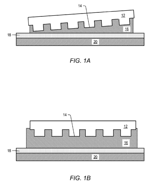
As is well known in the art, transfer layer 18 may allow one to obtain high aspect ratio structures (or features) from low aspect ratio imprinted features.
当分野で良く知られているように、転写層18により、低アスペクト比被転写フィーチャから高アスペクト比構造(すなわちフィーチャ)を得ることができる。
/////////
[0102] In an embodiment, a dispensed volume may typically be less than about 130 nl (nanoliter) for a 1 inch2 imprint area.
【0047】
一実施形態では、ディスペンスされる量は、通常、1インチ2の転写領域に対して約130nl(ナノリットル)未満である。
After dispensing, subsequent processes may involve exposing the template and substrate assembly to a curing agent.
ディスペンスが終了すると、次のプロセスには、テンプレートおよび基板のアセンブリを硬化剤に露出させるステップが含まれている。
Separation of the template from the substrate may leave a transferred image on top of the imprinted surface.
テンプレートと基板を分離させることにより、被転写表面の頂部に転写イメージが残される。
The transferred image may lie on a thin layer of remaining exposed material.
転写されたイメージは、残留している露出材料の薄層上に残される。
The remaining layer may be referred to as a “base layer.”
残留層は、「ベース層」と呼ばれている。
The base layer should be thin and uniform for a manufacturable imprint.
ベース層は製造可能転写のためには、薄く、かつ、一様でなければならない。


