和英特許翻訳メモ

便利そうな表現、疑問、謎、その他メモ書き。思いつきで書いてます。
拾った用例は必ずしも典型例、模範例ではありません。

の配置により

2020-10-31 22:21:30 | 英語特許散策

ES2763211
The processing elem ent can be configured to compare the signal generated by the disposition of(*の配置により)sensors with a known profile of one or more samples previously diagnosed.

US2018339338
32. A method of additive manufacturing a bulk amorphous metal part comprising:

providing a metallic glass forming alloy based on a metallic glass-forming alloy system with at least one component from the early transition metals and at least one other component from the non-early transition metals where a eutectic exists between the at least two components that results in a eutectic metallic glass forming alloy having a critical casting thickness, and wherein the amount of at least the components from the early transition metals of the metallic glass-alloy system are increased at the expense of the sum of the other components such that the metallic glass forming alloy is hypoeutectic and has a critical casting thickness less than the eutectic metallic glass forming alloy;
disposing(*配設、配置)molten layers of the hypoeutectic metallic glass forming alloy onto a build plate atop one another additively, and allowing said layers to cool to a bulk amorphous metal part having an amorphous fraction of at least 10% by volume, having an overall thickness of at least 1 mm, and having a density of at least 99.8%;
wherein the disposition occurs at a rate to prevent annealing of each disposed layer by the disposition of(*の配置、配設により)an overlaid layer; and
wherein the early transition metal components of the metallic glass forming alloy comprise at least 70% atomic the metallic glass forming alloy.
 
US7455925
There are several advantages of a layered fuel cell formed using sequential disposition of functional regions. One of the key advantages is the ability to dispose(*配置、配設)very thin layers. The advantages of thin layer fuel cells include: increased volumetric power density, improved heat and mass transfer, reduced losses through reduction of conductive path lengths, and potential cost reduction from a reduction in material requirements.
 
The present invention describes embodiments of the thin layer fuel cell structure in which the overall high aspect ratio structure is built-up by the disposition of(*の配置、配設により)functional regions in a sequential manner. The formation by sequential disposition eliminates the requirement for fabrication processes that can fill high aspect ratio structures.
 
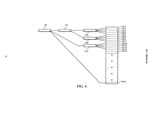
FIG. 10 illustrates details regarding the steps employed when placing files in the segments of a storage medium in accord with the present invention. To simplify the flow chart in FIG. 10, only files are mentioned; however, the logic disclosed therein applies equally to placing folders in segments. A decision step 300 determines if a file that is being placed will fit in an available space in a current segment that is being filled with folders and files. Segments are defined by the disposition of(*の配置、配設により)placeholders, as explained above. The available space would be between either an inner or outer limit of the storage medium layer and a placeholder, or between two successive placeholders. If the file will fit within the current segment being filled, a step 302 simply places the file within the current segment, immediately after the file that was placed just previously(*直前に). Thereafter, the process of placing the current file is completed, and the logic returns to the steps in FIG. 9. However, if a file currently being placed will not fit in the available space of the current segment, a decision step 304 determines if the placeholder that defines the remaining available space can be moved outwardly to abut against the files that were previously placed.
コメント
  • Twitterでシェアする
  • Facebookでシェアする
  • はてなブックマークに追加する
  • LINEでシェアする

広く適用できる

2020-10-31 15:49:10 | 英語特許散策(クレーム、通信)

EP2589834
[0020] While the advantages of the present invention as described herein will be described in part with reference to a vibration isolator strut (an exemplary structural member) of a vibration isolation system,
  [0020]ここで説明される本発明の利点は、振動分離システムの振動分離ストラット(例示的な構造的部材)に関して部分的に説明されるが、

the teachings of the present invention are generally applicable to any structural member having collinear threaded axial end portions,
本発明の教示は、同一線上のネジ付き軸方向端部を備える任意の構造的部材に広く適用でき

one threaded axial end portion being reverse threaded so that a length A (See FIG. 5) of the structural member is adjustable to substantially zero strain when mounting between a pair of opposed mounting brackets.
一方のネジ付き軸方向端部は逆ネジであり、構造的部材の長さAが、対向する取り付けブラケットのペアの間に取り付けられるときに実質的にゼロひずみに調整できるような任意の構造的部材に広く適用できる

EP2013109744
Example aspects of the method 300 as described relate to prerendering of a single page associated with a single navigation event,
方法300の例示的態様は、単一のナビゲーションイベントに関連付けられる単一のページのプリレンダリングに関連するが、

but the method 300 is also broadly applicable to prerendering multiple pages associated with one or more navigation events, such as prerendering multiple pages in sequence or in a plurality of parallel prerendering instances .
方法300は、順次的な複数のページのプリレンダリングまたは複数の並行したプリレンダリングインスタンスの複数のページのプリレンダリング等の、1つ又は複数のナビゲーションイベントに関連付けられた複数のページをプリレンダリングすることにも広く適用可能である。

EP2017203512
 While the described method is being described as being performed on one particular type of laser additive manufacturing process,
記載される方法は、1つの特定のタイプのレーザ付加製造プロセスで実行されるものとして記載されているが、

it is contemplated that this calibration method is broadly applicable to other additive manufacturing processes that utilize the skywriting process to control the switching on or off and scanning of a high energy beam during an additive manufacturing process.
この較正方法は、付加製造プロセス中にスカイライティングプロセスを利用してスイッチオン又はオフ、及び高エネルギービームの走査を制御する他の付加製造プロセスに広く適用できることが企図される。

コメント
  • Twitterでシェアする
  • Facebookでシェアする
  • はてなブックマークに追加する
  • LINEでシェアする

平準化する

2020-10-31 13:43:44 | 英語特許散策

EP3576505
[0017] In some embodiments the tongue is welded to both sides of the groove, forming a "double shear" weld joint.
【0017】
  いくつかの実施形態において、タングは、溝の両側に溶接され、「二面剪断」溶接接合を形成する。

The double shear weld joint balances applied forces during welding so stresses and deformation are equally distributed on each side of the tongue.
二面剪断溶接接合は、溶接中に印加される力を平準化するので、応力および変形は、タングの各側面に均等に分配される。

As a result, the double shear joint can result in less distortion of the cover and housing during joining, may require less fixturing to keep the cover and housing from distorting during the joining process
その結果、二面剪断接合により、接合中のカバーおよびハウジングの歪みが少なくなり、接合工程中にカバーおよびハウジングが歪まないように保つために必要な固定具を減らすことができ、

and may also form a stronger joint than a single sided shear joint.
片面剪断接合よりも強い接合を形成する。

EP3114202
[0052] Without wishing to be bound by theory, it is believed that solvents with relatively higher Hansen solubility values tend to migrate through water soluble film at greater rates and levels than solvents with relatively lower Hansen solubility values.
【0052】
  理論に束縛されるものではないが、比較的高いハンセン溶解度の値を有する溶媒は水溶性フィルムを通して、比較的低いハンセン溶解度の値を有する溶媒よりも、より高速かつ多量に移動して平準化する傾向があると考えられている。

Such solvents, then, induce migration of components from the liquid into and through the film.
次いで、このような溶媒は液体からフィルム内へ、かつフィルムを通しての、成分の移動を誘発する。

As a unit dose manufacturer generally seeks to minimize migration through film, it is thus counter-intuitive to select a solvent with relatively high Hansen solubility, for example, greater than 29.
単位用量製造者は通常、フィルムを通しての移動を最小限にしようと努めるため、比較的高い、例えば29より大きいハンセン溶解度を有する溶媒を選択することは、反直観的なことである。

WO2014043420
[00129] Transmission of data across various channels may be limited by various constraints.
【0129】
  様々なチャネルによるデータ送信は、様々な制約により制限される。

For example, in one embodiment, this may be done by fiber-optic channels, and here, transmission speeds may be limited by the speed of light through the medium of the channel.
例えば1実施例において、これは光ファイバチャネルによりなされる。

In such an embodiment, the time to travel is calculated by dividing the distance that must be traversed by the speed of light through the medium.
この場合、通信速度はチャネル媒体を介して光速度により制限される。この実施形態において、伝搬時間は伝搬距離を媒体の光速度で除算することにより求められる。

Accordingly, the time to travel can be equalized by adding additional length to the medium or changing the medium.
したがって伝搬時間は、媒体に距離を追加するかまたは媒体を変更することにより、平準化することができる。

Equalizing the length of the medium of transmission by adding length to the shorter channels may allow for simultaneous delivery of information.
短いチャネルに対して距離を追加することにより送信媒体の長さ平準化すると、情報を同時配信することができる。

In some embodiments, this may guarantee simultaneous delivery within nanoseconds.
実施形態において、これはナノ秒以内の同時配信を保証する。

WO2019014277
To be compatible with all types of wireless signal transmitters,
全てのタイプの無線信号送信機と適合するように、

an initial calibration for each transmitter with respect to the system is required to level out the effect of different types of signal transmitters for better accuracy in determining the distance and the angle of the system with respect to the target.
標的に関してシステムの距離および角度を決定する際により優れた精度のために異なるタイプのシグナル送信機の効果平準化するために、システムに関するそれぞれの送信機に対して初期校正が必要とされる。

WO2018226600
[0049] These tests, taken together, smooth out some of the moment-to-moment fluctuations in the RSSI radio signal strength of the BLE devices,
【0043】
  これらの試験を組み合わすことによって、BLE装置のRSSI無線信号強度における瞬間的な変動の一部平準化するのに役立ち、

thereby adding a greater degree of certainty as to the proximity of the user being within 0-3 meters of the SmartBeacon device
これによってユーザの近接度により高い確度を付し、これはユーザがスマートビーコン装置の0~3メートル以内にあるか否かに関するものであり

and in all likelihood in front of the SmartBeacon device rather than to its side or behind it (the antenna on the SmartBeacon device is slightly directional).
即ちスマートビーコン装置の横や背後ではなくその前に存していることがかなり確かであるか否かに関するものである(スマートビーコン装置のアンテナは幾ばくかの指向性を有している)。

WO2018048993
[0042] The inclusion of the recirculation channel 236 in the applicator 10 helps alleviate this issue.
【0034】
  再循環チャネル236がアプリケーター10内に含まれることは、この問題を軽減するのに役立つ。

When the valve stem 260 is in the second position, the ability of the adhesive to flow from the central section 224b of the dispensing flow path 224 to the upper section 224a, and through the recirculation feed channel 232 to the recirculation channel 236 provides the adhesive the ability to escape the dispensing flow path 224.
バルブステム260が第2の位置にあるとき、接着剤が吐出流路224の中央セクション224bから上側セクション224aに流れ、再循環供給チャネル232を通って再循環チャネル236へと流れる能力は、接着剤に吐出流路224から脱出する能力を与える。

This may alleviate any pressure build-up that could occur when the valve stem 260 is in the second position,
これにより、バルブステム260が第2の位置にあるときに生じ得る圧力の上昇を軽減し、

thus aiding in standardizing the flow of adhesive through the nozzle 21 when the valve stem 260 is in the first position.
したがって、バルブステム260が第1の位置にあるときにノズル21を通る接着剤の流れ平準化することに役立つことができる。

WO2018044662
Bidimensional measurements of tumors are performed twice a week and tumor volumes are calculated based on the following formula: (Tumor Volume) = [(L) x (W2) x (Π/6)] where L is mid-axis length and W is mid-axis width.
腫瘍の2次元測定を週2回実施し、以下の式:(腫瘍体積)=[(L)×(W2)×(Π/6)]に基づいて腫瘍体積を算出し、上式では、Lは中軸長であり、Wは中軸幅である。

Tumor volume data are transformed to a log scale to equalize variance across time and treatment groups.
腫瘍体積データをlogスケールに変換して、時間および処置群にわたる分散平準化する

The log volume data are analyzed with a two-way repeated measures analysis of variance by time and treatment using the MIXED™ procedures in SAS™ software (version 8.2). 
SAS(商標)ソフトウェア(バージョン8.2)のMIXED(商標)工程を使用して、時間および処置による分散の2元配置反復測定分析を用いて、log体積データを解析する。

WO2018027100
For example, continuous reinforcement can be provided by web 26 or a roll (not shown) upstream to the headbox in addition to that providing web 26 to lay the continuous reinforcement above web 26.
例えば、連続強化剤は、ウェブ26を提供するロールに加えて、ウェブ26またはロール(図示せず)によってヘッドボックスの上流に提供して、ウェブ26の上に連続強化剤を置くことができる。

To assist in leveling the fiber-slurry mixture 46 a forming vibrating plate 50 may be provided under or slightly downstream of the location where the forming assembly 40 deposits the fiber-slurry mixture 46.
繊維スラリー混合物46平準化するのを支援するために、形成振動プレート50を、形成アセンブリ40が繊維スラリー混合物46を堆積させる場所の下に、またはわずかに下流に提供することができる。

WO2008006647
Unlike the Token Bucket, packets are allowed to filter out of the "leaky" bucket at a constant rate of / bytes per second.
トークン・バケットと異なり、「リーキー」バケットからlバイト/秒の一定レートでパケットをフィルタさせることができる。

Such filtering imposes a hard limit on the data transmission rate (by enforcing space between packets) and produces the effect of smoothing out bursty data.
かかるフィルタリングは、(パケット間のスペースを強制することにより)データ伝送レートにハード制限を課し、バースト性データを平準化する効果をもたらす。

WO2005050448
Write data from the first redrive circuit 60 is accumulated in the write FIFO at whatever data rate the outbound path happens to be operating at.
【0101】
  第1の再駆動回路60からの書き込みデータは、アウトバンド経路が動作している何れのデータ・レートでも書き込みFIFOに蓄積される。

Once enough write data is accumulated, it may be written to one or more memory devices at full burst rate through memory bus 68.
書き込みデータは、十分蓄積されると、完全なバースト・レートでメモリ・バス68を介して1つ又は複数のメモリ装置に書き込み得る。

The read FIFO 194 may perform data capture from the memory device at full burst rate, and levelize the data prior to transferring the read data to the second redrive circuit 62 through multiplexer 74. 
読み取りFIFO194は、メモリ装置からのデータ捕捉を完全なバースト・レートで行い、読み取りデータを第2の再駆動回路62にマルチプレクサ74を介して転送する前にデータを平準化し得る。

WO2008154214
[0008] In a second aspect of the invention, a method includes receiving a series of signals, and equalizing the received signals using an equalization value.
【0008】
  本発明の第2の特徴は、一連の信号を受信し、平準化値を使って受信データを平準化することを有することである。

A clock signal is generated based at least in part on a bandwidth value, and the received signals are over-sampled using the clock signal.
クロック信号は、少なくとも部分的に帯域幅値に基づいて生成され、受信信号は、このクロック信号を使ってオーバーサンプリングされる。

The equalization and eye quality of the received signals are monitored, and possible values of parameters are scanned.
この平準化及び受信データの監視品質はモニターされ、可能なパラメータ値がスキャンされる。

A combination of parameters for data reception is identified.
データ受理に対するパラメータの組み合わせが識別される。

コメント
  • Twitterでシェアする
  • Facebookでシェアする
  • はてなブックマークに追加する
  • LINEでシェアする

から照射された光

2020-10-30 16:57:02 | 英語特許散策

WO2016109026
[0030] With reference to Figure 7, light source 38 illuminates tape 10 with a first light beam 60 at a first angle of incidence θπη to generate an image of the tape surface by direct reflection.
【0018】
  図7を参照すると、光源38は、第1の入射角θ1inで第1の光ビーム60によってテープ10を照射して、直接反射によってテープ表面の画像を生成する。

As depicted in Figure 7, light source 38 illuminates tape 10 from below.
図7に示すように、光源38は下からテープ10を照射する。

Since the tape is visualized by direct reflection, θπη equals the angle of reflection 0l out of reflected light beam 62.
テープは直接反射によって映像化されるため、θ1inは反射光ビーム62の反射角θ1outに等しい。

Light emitted from light source 38 reflects off of mirror 64 onto the tape surface. 
光源38から照射された光はミラー64で反射してテープ表面に当たる

WO2016043986
[0045] In some embodiments, the target 48 may include one or more regions (e.g., 1, 2, 3, 4, 5, 6, 7, 8, or more) representative of the alignment status of the turbine trailer 20.
【0037】
  実施形態によっては、ターゲット48は、タービントレーラ20の整列状態を代表する1つ又は複数(例えば、1、2、3、4、5、6、7、8、又はそれより多く)の領域を含むことがある。

For example, the target 48 may include a first region 48a, a second region 48b, a third region 48c, a fourth region 48d, and a fifth region 48e indicative of the alignment statues.
例えば、ターゲット48は、整列状態を代表する第1の領域48a、第2の領域48b、第3の領域48c、第4の領域48d、及び第5の領域48eを含むことがある。

In some situations, the beam of light 101 emitted from the laser 46 may hit the target 48 in the first region 48a or the second region 48b,
状況によっては、レーザ46から照射された光ビーム101は、第1の領域48a又は第2の領域48b内のターゲット48に当たることがあり、

which may indicate that the alignment status of the turbine trailer 22 may be approximately bent in a horizontal direction 57, such as in the left lateral direction 112. 
それは、タービントレーラ22の整列状態が左横方向112などの水平方向57に略曲がっているかもしれない、ということを示すことができる。

WO2014160058
[0021] In Figures 3 and 4, at least one lens 221 is integral to or directly fixed to wall 212 or 216, for example, and performs functions in addition to those described above.
【0021】
  図3と図4では、少なくとも一つのレンズ221が、例えば壁212又は壁216に埋め込まれているか、又は直接固定されており、上記の機能に加えて別の機能を果たしている。

At least one lens 221 is arranged to transmit light 230 to space 220, or receive light 230 transmitted through space 220 and transmit light 230 to lens 224.
少なくとも一つのレンズ221は、空間220へ光230を照射するために、又は空間220を通過して照射された光230を受光してレンズ224へ光230を照射するために、配置されている。

In the example of Figures 3 and 4, lens 221A and 221B are positioned on wall 216 and arranged to receive light 230 transmitted through space 220 and
図3と図4の例では、レンズ221Aとレンズ221Bはそれぞれ、壁216に位置しており、空間220から照射された光230を受光し、

focus and transmit the received light to lens 224A and 224B, respectively.
レンズ224Aとレンズ224B受光した光の焦点を合わせ照射するために配置されている。

WO2011011213
Figure 3 A is similar to Figure 2A, but it shows developer liquid 108 depleted to a level that fresh developer liquid is needed to be replenished into tank 104.
【0015】
  図3Aは図2Aに類似しているが、タンク104に未使用現像液を補充しておく必要がある液位まで現像液108を消費してしまった場合を示している。

The light beam emitted from light emitter 232 hits reflective surface 204 in direction 220. 
光エミッタ232から照射された光ビームは、方向220にある反射面204に当たる。

US2009161197
With this in mind, shown in FIG. 3A is a ROS system 10
【0024】
  これを念頭に、図3AはROSシステム10を示す。

which includes a light source such as laser 12, the agile beam steering mirror assembly 14 according to the present invention,
これはレーザ12等の光源と、本発明に係る走査ビームステアリングミラーアセンブリ(agile beam steering mirror assembly)14と、

a rotating polygon mirror assembly 16, scan optic assembly 18, mirror 20, and photoreceptive drum 22.
回転式ポリゴンミラーアセンブリ16と、走査光学アセンブリ18と、ミラー20と、光受容体ドラム22とを含む。

Following the path of light emitted from laser 12, a light beam is incident on agile beam steering mirror assembly 14 which adjusts the beam position as described further below. 
レーザ12から照射された光の通路に従って光ビームを走査ビームステアリングミラーアセンブリ14に入射する。

コメント
  • Twitterでシェアする
  • Facebookでシェアする
  • はてなブックマークに追加する
  • LINEでシェアする

後に詳しく説明

2020-10-30 13:53:08 | 英語特許散策

EP3294170
[0015] Fig. 3 shows cross-section 3A-3A of Fig. 2A. As shown, located within the catheter shaft 16 is a pressure detecting tube 26.
【0015】
  図3は、図2Aの3A-3A断面を図示している。図示されているように、前記カテーテル軸16内には、圧力検出チューブ26が配設されている。

The cavity between the inner wall of the catheter shaft and the outer wall of the pressure detecting tube
カテーテル軸の内壁と前記圧力検出チューブの外壁との間のキャビティは、

defines an exhaust lumen 28 for the passage of gases from the balloon interior for discharge through the connector 22 and exhaust assembly 108, which will be discussed in greater detail below.
後に詳しく説明するように、排出のためにバルーン内部から前記コネクタ22と排出アセンブリ108とを通って気体を通過させるための排出ルーメン28を形成する。

The pressure detecting tube 26 includes a circular central lumen containing a delivery tube 30.
前記圧力検出チューブ26は、デリバリチューブ30を包含する円形中央ルーメンを有する。

The cavity between the inner wall of the pressure detecting tube 26 and the outer wall of the delivery tube 30 defines a pressure detecting lumen 32 used to detect the static pressure within the balloon 24.
前記圧力検出チューブ26の内壁と前記デリバリチューブ30の外壁との間のキャビティは、前記バルーン24内の静圧を検出するために使用される圧力検出ルーメン32を形成する。

EP2905118
In one aspect of the disclosure, which may include at least a portion of the subject matter of any of the preceding and/or following examples and aspects,
上述および/または後述する例及び態様の要旨の少なくとも一部を含み得る本開示の一態様において、

the path 400 is a spiral path that serves to accommodate, inter alia, central placement of a heating element (described in detail below) inside the extrusion nozzle 300,
通路400は螺旋形の通路であり、これによって、とりわけ加熱エレメント(後に詳しく説明する)を押し出しノズル300内の中央に配置することができ、

making the assembly more compact and promoting uniform heat distribution within the extrusion nozzle 300.
装置をより小型化し、押し出しノズル300内において熱を均等に分散させることができる。

US8361018
In at least one embodiment, the configuration of the syringe assembly
少なくとも1つの実施形態において、シリンジアセンブリの構成により、

allows for the flexible protrusion 444 to advance distally past the rib 423, to lock the plunger rod 440 in the barrel 420, when the user bottoms the syringe assembly (as more clearly shown in FIGS. 37-38 and discussed further below).
使用者がシリンジアセンブリを最後まで押し切ると、柔突起444は隆起部423を越えて遠位方向に進み、押子440が外筒420の中にロックされる(図37~図38により明瞭に示し、後に詳しく説明する)。

The plunger rod may further include an optional pair of discs 430, 431 disposed on the distal end and proximal end of the main body 448.
押子はさらに、主要部448の遠位端と近位端に配置された、任意の1対のディスク430、431を含んでいてもよい。

The discs 430, 431 provide additional stability and may have alternate shapes, depending on the shape of the barrel.
ディスク430、431により安定性が増し、これらは外筒の形状に応じて、別の形状であってもよい。

コメント
  • Twitterでシェアする
  • Facebookでシェアする
  • はてなブックマークに追加する
  • LINEでシェアする

説明するための図

2020-10-30 10:32:14 | 英語特許散策

US2017068423
 Further, in examples where the digital assistant is invoked while displaying passive visual indicator 606 (e.g., FIG. 6E),
更に、受動的視覚的インジケータ606(例えば、図6E)を表示している間にデジタルアシスタントが呼び出される実施例では、

the display of visual indicator 606 can be replaced with the display of active visual indicator 614.
視覚的インジケータ606の表示を能動的視覚的インジケータ614の表示と置換することができる。

This can provide a natural transition from the instructive user interface shown in FIGS. 6B-E for demonstrating how to invoke and interact with the digital assistant to the active user interface shown in FIG. 6F for actively interacting with the digital assistant.
これは、どのようにデジタルアシスタントを呼び出し、それと対話するのかを実例説明するための図6B〜図6Eに示される教示的なユーザインターフェースから、デジタルアシスタントと能動的に対話するための図6Fに示される能動的ユーザインターフェースへの自然な移行を提供することができる。

WO2018195461
[0076] FIG. 9 describes an exemplary method of signals that may invalidate an anticipated motion vector set. 
【0063】
  図9は、予測された動きベクトルセットを無効にすることのできる信号の例示的な方法を説明するための図である。

WO2018156486
[0027] Figure 5A is a diagram to illustrate a method for determining a capacitance Cseries of a series circuit of an impedance matching circuit and a capacitance Cshunt of a shunt circuit of the impedance matching circuit to reduce reflected power at an output of an RF generator for the states S(n-N) through S(n).

【図5A】状態S(n-N)~S(n)に対してRF発生器の出力での反射電力を削減するためにインピーダンス整合回路の直列回路の静電気容量Cseriesと、インピーダンス整合回路のシャント回路の静電容量Cshuntとを決定する方法を説明するための図

EP3361224
[0019] The features, functions and advantages discussed in the preceding section can be achieved independently in various embodiments
【0018】
  前のセクションで論じた形態、機能、および利点を、様々な実施形態において独立して達成することができ、

or can be combined in yet other embodiments.
またはさらに他の実施形態で組み合わせてもよい。

Various embodiments will be hereinafter described with reference to drawings for the purpose of illustrating the above-described and other aspects.
上記およびその他の態様を説明するための図を参照しながら、以下に様々な実施形態について説明する。

WO2012087403
Figure 1 A illustrates a conventional MOS device that includes source and drain tip regions formed using implantation and diffusion.
【図1A】注入処理および拡散処理を利用して形成されるソース先端領域およびドレイン先端領域を含む従来のMOSデバイスを示す図である。

Figure IB illustrates a MOS device that includes source and drain epitaxial tips configured in accordance with an embodiment of the present invention.
【図1B】本発明の実施形態に応じた構成のソースエピタキシャル先端部およびドレインエピタキシャル先端部を含むMOSデバイスを示す図である。

Figure 1C illustrates how spacer thickness can impact etching of epitaxial tips of a MOS device.
【図1C】スペーサの厚みがMOSデバイスのエピタキシャル先端部のエッチングに影響を与える様子を示す図である。

Figure ID is a graph illustrating the dependence of UC-to-UC distance on spacer thickness.
【図1D】スペーサの厚みに対するUC間距離の依存性を説明するためのグラフである。

Figure 2 is a method of forming source and drain epitaxial tips in accordance with an embodiment of the present invention.
【図2】本発明の実施形態に応じたソースエピタキシャル先端部およびドレインエピタキシャル先端部を形成する方法を示す図である。

Figures 3A to 3 J illustrate structures that are formed when carrying out the method of Figure 2, in accordance with various embodiment of the present invention.
【図3A】本発明のさまざまな実施形態に応じて図2の方法を実行する際に形成される構造を示す図である。

General Overview
【0005】
  <概論(*概略、まとめ)

...

Figures 6 A and 6B further demonstrate improvements enabled by using self-aligned source and drain epi-tips configured in accordance with one example embodiment of the present invention.
図6Aおよび図6Bはさらに、本発明の一実施形態例に応じて構成された自己整合型のソースエピ先端部およびドレインエピ先端部を用いることで可能となる改善点をさらに説明するための図である。

EP1198070
FIG. 1 is a block diagram of a first configuration of a networked sound system according to the invention;
【0016】
【図1】本発明によるネットワーク・サウンド・システムの第1の構成のブロック図である。

FIG. 2 is a block diagram of a second configuration of a networked sound system according to the invention;
【図2】本発明によるネットワーク化されたサウンド・システムの第2の構成のブロック図である。

FIG. 3 is a block diagram of the interface unit of FIGS. 1 and 2;
【図3】図1および図2のインターフェース・ユニットのブロック図である

FIG. 4 is a diagram helpful in explaining the logical database relationships of recorded units and assemblages of recorded units;
【図4】記録済みユニットおよび記録済みユニットの集合の論理的なデータベース関係を説明するための図である。

FIG. 5 is a sound reproduction device control panel according to the invention;
【図5】本発明による音響再生装置コントロール・パネルの図である

FIG. 6 is a representation of an interface screen on a computer display in accordance with the invention;
【図6】本発明によるコンピュータ・ディスプレイ上のインターフェース画面の表示である。

FIG. 7 is a flow diagram for assigning broadcast radio frequencies to the preset buttons according to the invention;
【図7】本発明による放送ラジオ周波数をプリセット・ボタンに割り当てる流れ図である。

FIG. 8 shows the buttons on the remote control device;
【図8】遠隔制御装置上のボタンを示している

FIGS. 9A, 9B, 9C and 9D are schematic circuit diagrams of circuitry in a radio that implement elements 12, 14 and 16 of the system of FIG. 2;
【図9】図2のシステムの要素12、14および16を実施するラジオにおける回路の略回路図である

WO2018085237
[0031] FIG. 3 is an enlarged view of the portion A of FIG. 1A, for explaining an operation of selecting a gradient of an illumination optical system;
【図3】照明光学系の勾配を選択する動作を説明するための1AのA部分の拡大図である。

WO2017165206
Figures 3A and 3B describe an exemplary fabrication process 300 of fabricating the interconnect structure 200 and the self-aligned via 212(1) that is self- aligned to and interconnected between a respective underlying metal line 208(1) and overlying metal line 210(1) of the interconnect structure 200 in Figures 2A and 2B.
図3Aおよび図3Bは、相互接続構造200を製作し、かつ図2Aおよび図2Bにおける相互接続構造200のそれぞれの下部金属線208(1)および上部金属線210(1)に自己整合し、下部金属線208(1)と上部金属線210(1)との間に相互接続された自己整合ビア212(1)を製作する例示的な製作プロセス300について説明するための図である。

WO02069030
Figure 5A illustrates an effect of providing one light modulator which has lower resolution than another light modulator;
【図5A】他の光変調器よりも低い分解能を持つ光変調器を備えることの影響を説明するための図

コメント
  • Twitterでシェアする
  • Facebookでシェアする
  • はてなブックマークに追加する
  • LINEでシェアする

device whereby/with which

2020-10-29 23:26:45 | 英語特許散策

US8789939(Google)
In use, the cartridge of the invention is inserted into an appropriately configured printer device whereby(*先行詞は前文)the drive gear 21 aligns with and engages a corresponding driven gear provided on the printer mechanism. The advantages of this configuration are numerous. Most importantly, the provision(*設ける)of the transportation means within the cartridge ensures that the paper or other print media is fed out of the cartridge accurately and with minimum initial contamination, as the mechanism and print media are housed within an enclosed unit. In cartridges of the prior art, the cartridge is pressed onto a pick up roller mounted in the printer device, which exposes the paper on the underside(*裏側、裏面、背面). By contrast, the present design allows for greater structural integrity as(*なので、ため、理由、because)there is no need to provide an opening that exposes the print media to that same extent. Further, the design provides for(*もたらす、得る事を可能)a tamper proof unit.

US8391719(Google)
Abstract
Methods and systems for conducting communication(*通信を行う)between mobile devices are disclosed herein. In one embodiment, a method of achieving communications(*通信を達成)between first and second mobile devices that are in proximity with one another includes transmitting a first signal from the first mobile device and receiving a first reflected signal at that(*その、前記、同、該、当該)mobile device, the first reflected signal being the first signal reflected by an object in proximity to that mobile device. The method also includes transmitting a second signal from the first mobile device for receipt by the second mobile device upon being reflected by the object, and receiving a confirmation signal from the second mobile device in response to the second signal. The method further includes achieving a paired relationship of the first mobile device relative to the second mobile device, whereby(*achievingに係る、so that)because of the paired relationship the first and second mobile devices are capable of additional communications therebetween.

US10582464(Google)
The new master device 305 can establish 330 an additional audio playback session with the new slave device 304, similar to 230 as discussed with respect to FIG. 2. The new master device 305 can send 332 a portion of the additional audio file to the new slave device as well as a new timing instruction using the additional audio playback session, whereby(*whereinの方が良い?)the new timing instruction can include a current system time of the new master device 305. The new master device 305 can initiate 334 playback of the additional audio file and the new slave device 304 can initiate 336 playback of the additional audio file according to the new timing instruction as well as the new system clock offset value resulting from 350, similar to 234 and 236 as discussed with respect to FIG. 2. Thus the old slave device 305 becomes the new master device whereby(*その結果、so that, such that)the playback commands 242, the sync confirmations 240241, and the additional audio file portions transmittals 238 are still active, but now for the new master device.

US8958018(Google)
15. The method according to claim 8, further comprising the step of displaying media on the primary display screen under control of the primary electronic device that is uninterrupted during said steps of transmitting information to the secondary device, displaying the information on the secondary display screen, and collecting user input on the secondary device whereby(*先行詞はdeviceではない)the display of media on the primary display screen remains uninterrupted until an operational command is transmitted.

US7228418(Google)
When the Transferring Node transfers a session to the Target Node, all of the Transferring Node's IP traffic is transferred to the Target Node. This is convenient when a session has multiple flows, as(*なので、理由、because)all of the flows are transferred together. However, if the Transferring Node simultaneously has other active sessions, they will also be transferred. For simple devices that only have one active session at a time, such as a wireless videophone, this may not be an issue. However, for more complex services, a method and apparatus supporting a plurality of IP addresses at the first destination device whereby(*先行詞はmethod and apparatus;複数のアドレスをサポートする方法および装置であって、該複数のアドレスのうち1つが~される方法および装置が望ましい)a unique IP address from the plurality of IP addresses is assigned to a unique transferable session may be desirable. Such a system is depicted in FIG. 2 and FIG. 2 b.

AU2008205032(Apple)
A user of the host computer 1302 can select and play back a media asset stored within the host data storage device 1310 through use of(*を用いて)the media management application 1308. Typically, the host computer 1302 will include or couple to a display device whereby(*前文全体なら=so that, display deviceなら=such that)the playback of the media asset can provide visual media output (e.g., display device) and/or audio media output (e.g., a speaker). The display device can also support a graphical user interface that provides menus, user interface (UI) controls, etc. that assist a user in interacting with the host computer 1302 while selecting and playing media assets.


wherebyは直前の名詞に係る場合よりも前文全体に係り結果や目的(so that, such that)を表す場合が多い?

US9317709(Google)
Abstract
A cloud storage system(*不定冠詞だが本発明の)provides remote access to a file associated with the cloud storage system. In response to a request to access the file, the cloud storage system identifies applications available to the request generator and capable of accessing the file, which may include both online web-based applications and applications installed on a device with which(*を用いて、手段)the user is accessing the file. The cloud storage system determines an application type of an identified application, and provides file access to the identified application based on the application type.

US10257686(Google)
12. The electronic device of claim 10, wherein the instructions are configured to cause the one or more processors to:

authenticate identity of the electronic device by sending a device identifier for the electronic device to the commissioning device with which(*を用いて、手段;先行詞はdevice identifier)the electronic device verifies identity upon connection to the commissioning device; and
establish a secure communication session with the commissioning device using the device identifier, the secure communication session being established through a secure tunnel and via an assisting device.
コメント
  • Twitterでシェアする
  • Facebookでシェアする
  • はてなブックマークに追加する
  • LINEでシェアする

毛髪の量

2020-10-29 19:52:15 | 英語特許散策

WO2018213651
Hair volume
【0071】
  毛髪の量

(i) Preparation of hair switch
(i)ヘアピースの準備
 
For the volume measurement, 15 gram hair switch with a length of lOinch are used. The hair switches are prepared by following steps:
体積の測定には、長さ10インチの、15グラムのヘアピースを使用する。ヘアピースは以下の工程により準備する。
 
Silicone extraction
【0159】
シリコーンの抽出
 
For each hair tress, 100ml polyethylene bottles were tarred.
各毛束のために、100mlのポリエチレン瓶の風袋を秤量した。
 
The hair tress was introduced in the bottle while maintaining the mounting tab outside the bottle.
瓶の外部の取り付けタブ(mounting  tab)を維持しながら、瓶の中に毛束を入れた。
 
The hair was cut just below the mounting tab and the amount of hair introduced in the bottle was recorded.
取り付けタブのすぐ下で毛髪をカットし、瓶の中に入れた毛髪の量を記録した。
コメント
  • Twitterでシェアする
  • Facebookでシェアする
  • はてなブックマークに追加する
  • LINEでシェアする

単位ユニット

2020-10-29 19:24:44 | 英語特許散策

WO2007025146
Pharmaceutical preparations, in the form of, for example, tablets, caplets, and capsules may contain from about 100 mg to about 1400 mg of the pharmaceutical composition (i.e., balsalazide and excipient(s)), more preferably from about 700 mg to about 1200 mg of the composition.
【0054】
  医薬製剤は、例えば、錠剤、カプレット、およびカプセルの形態で、医薬組成物の約100mg~約1400mg(即ち、バルサラジドおよび賦形剤(単数または複数))、より好ましくは組成物の約700mg~約1200mgを含んでもよい。

Specific single unit dosage forms of the invention contain 50, 100, 150, 200, 250, 300, 350, 400, 450, 500, 750, 1000, 1100, 1200, 1300, 2000, 2500, 3000, or 3300 mg of active ingredient. 
本発明の特定の単位ユニット剤形は、50、100、150、200、250、300、350、400、450、500、750、1000、1100、1200、1300、2000、2500、3000、または3300mgの有効成分を含む。

EP2807223
"polymer" means the polymerization product of one or more monomers and is inclusive of homo-, co-, ter-, tetra-polymers, etc.;
  「ポリマー」は1種以上のモノマーの重合生成物を意味し、ホモ-、ジ-、ター-、および、テトラ-ポリマーなどを含む。

"mer" or "mer unit" means that portion of a polymer derived from a single reactant molecule (e.g., ethylene mer has the general formula— CH2CH2— );
「単量体単位」または「単量体単位ユニット(mer unit)」は、単一の反応体分子から得られたポリマーの部分を意味する。例えば、エチレン単量体単位は、一般式  -CHCH-  を有する。

WO2018108743
[0031] In connection with various embodiments of the present disclosure, low cost microbolometers today have pixel counts starting at 80 by 60 for a total of 4800 pixels.
【0020】
  本開示の各種実施例に関し、今日の低コストのマイクロボロメータは、80×60で始まり、全体で4800画素の画素カウントを有する。

Each pixel element is a temperature sensitive resistive material made from vanadium oxide or amorphous silicon.
各画素素子は、酸化バナジウムまたはアモルファスシリコンで構成された、温度検知抵抗材料である。

Microbolometers, once exclusively used in military applications have now been established in the commercial arena and have thus greatly been reduced in cost.
かつては軍用途に排他的に使用されてきたマイクロボロメータは、現在、市販されるようになり、従って、コストが大きく低減されている。

Like in the visible CMOS image sensor market, it is forecasted that pixel count and sensitivity for microbolometers will keep increasing as volume production increases with cost per unit decreasing.
CMOSイメージセンサの市場と同様、マイクロボロメータの画素カウントおよび感度は、単位ユニット当たりのコストの低下とともに大量生産が増え、上昇し続けることが予測されている。

EP2632613
[0078] In another embodiment depicted in Fig. 7b , at least a portion of the engineered surface 700 comprises a plurality of structure geometries.
【0075】
  図7bに示される別の実施形態において、加工表面700の少なくとも一部分は、複数の構造幾何形状を含む。

For example, a unit cell including a pyramidal projections is directly adjacent a unit cell including a post.
例えば、角錘の突出部を含む単位セルは、ポストを含む単位セルに直接隣接する。

Each unit cell is still defined at least partially by a dimension at least approximating, preferably equal to, the pitch and includes a single microstructure.
単位ユニットは、ピッチに近似する、好ましくは、それと同等の寸法によって、少なくとも部分的に更に画定され、単一のミクロ構造を含む。

WO2016039959
[00124] In the example shown, cabinet frame 1100 also includes reinforcing front-to-back beams 1145 to increase the overall rigidity of cabinet frame 1100, making electronics cabinet 1000 more resistant to impact deformation.
【0040】
  図示される実施例において、キャビネットフレーム1100はまた、キャビネットフレーム1100の全体の剛性を高めることで電子機器キャビネット1000の耐衝撃変形性を高める、補強前後梁1145を含む。

In the particular example shown, each of the reinforcing front- to-back beams 1145 consist of a three piece assembly and are welded, or otherwise securely fastened or connected, to between vertical posts 1125.
図示される特定の実施例において、補強前後梁1145のそれぞれは3部品のアセンブリから成り、垂直柱1125間に溶接されるか、または確実に固定されるか、もしくは接合される。

However, reinforcing front- to-back beams 1145 can also be a single, unitary unit
しかし、補強前後梁1145はまた、単一の単位ユニットであってもよい。

コメント
  • Twitterでシェアする
  • Facebookでシェアする
  • はてなブックマークに追加する
  • LINEでシェアする

2020-10-29 17:38:11 | 英語特許散策

US10271087
In some aspects, the media guidance application (or a user device upon which the media guidance application is implemented) may incorporate and/or have access to an electroencephalogram unit (“EEG”) indicating a first frequency range of voltage fluctuations in the brain activity of a user and/or an electromyogram unit (“EMG”) indicating first electrical activity of muscles near a brain(*不定冠詞)of the user at rest and during contraction. 

US10357660
SUMMARY OF THE INVENTION

Described herein, in certain embodiments, are methods and systems for modulating the electrical activity of a brain(*不定冠詞). Described are methods and devices for modulating the electrical activity of a brain that involve no medication. Methods and devices described herein gently “tune” the brain and affect mood, focus, and cognition of human subjects. Methods and devices described herein gently “tune” the brain and affect mood, focus, and cognition of subjects.

In one aspect are methods of modulating the electrical activity of a brain in a subject in need thereof, comprising: (a) adjusting output of a magnetic field for influencing an intrinsic frequency of a specified EEG band of the subject toward a target intrinsic frequency of the specified EEG band; and (b) applying said magnetic field close to a head(*不定冠詞)of the subject.

In another aspect are methods of altering an intrinsic frequency of a brain of a subject within a specified EEG band, comprising: (a) determining the intrinsic frequency of the subject within the specified EEG band; 

US20090005827

1. An apparatus for stimulating the neurochemistry of the brain(*定冠詞)of a subject, said apparatus comprising:

a goggle member including a pair of eye shields, said eye shields having a periphery;
at least one light disposed about said periphery of each of said eye shields a distance of between 1½ and 2½ inches from the retinas of the subject; and
circuit means to drive said at least one light at a frequency of between 1-1200 Hz.
 
    TECHNICAL FIELD
  • [0004]
    The present invention relates generally to the field of brain stimulation, and more particularly to increases in brain chemistry for enhancing overall brain function, including cognitive abilities and intelligence quota (IQ), utilizing full spectrum white light applied to both eyes or only to one eye, at frequencies ranging from 1-1200 Hz, omitting 55-65 Hz to avoid seizure. Both “fuzzy” light and “fuzzy” sound are an integral part of the method, and are controlled though computerized sessions, which can be downloaded to any existing light/sound device. More specifically, this is an apparatus and method for enhancing overall brain functions, including cognitive abilities and intelligence quota (IQ). Other treatment interventions this apparatus and method can positively affect include neurological, physiological, and psychological disorders and diseases.
  • BACKGROUND INFORMATION AND DISCUSSION OF RELATED ART
  • [0005]
    Brainwave states are derived from natural frequencies occurring within the cortex, but can be altered through the use of light and sound driven devices. When a light emitting goggle or light frame is worn over the eyes, any lights flickering at specific frequencies for a length of time will cause a reaction in brainwave activity. For example, if the light goggles are set to flicker at 13 Hz for a ten to twenty minute period of time, the brainwave activity will slow or become faster and match, or “entrain” to the 13 Hz frequency. This action is typically called “entrainment” or “frequency following response” (FFR). This is a common process utilized by most light/sound devices to guide the user into desired brainwave states.
  • [0006]
    Light and sound stimulation therapy utilizes a variety of light/sound devices, to alter brainwave activity, regulate circadian rhythms, and treat seasonal depressive disorder, for example. Light/Sound devices have been employed for improvements in relaxation, cognitive development, peak performance, problem solving abilities, and to increase test scores in learning disabled. children.
  • [0007]
    Previous animal studies have indicated that animals placed in enriched and stimulating environments result in higher learning and increases in brain weight and density. Effects of stimulation in the human brain(*定冠詞)have been positive. Postmortem human studies revealed that subjects exposed to challenging and stimulating environments demonstrate greater dendritic length and structural changes in the cortex.
Abstract
The present invention provides specific methods of using and administering etanercept to improve cognitive function in a human, for both the treatment and prevention of cognitive impairment, or, alternatively, to enhance cognitive function including Alzheimer's Disease, Idiopathic Dementia, and Traumatic Brain Injury. The methods of the present invention include the perispinal administration of etanercept. For the purposes of this patent “perispinal” is to be considered as referring to “perispinal extrathecal;” therefore direct intrathecal administration is excluded. Perispinal administration leads to enhanced delivery of etanercept to the brain(*初出で定冠詞)in a therapeutically effective amount, via the vertebral venous system and/or the cerebrospinal fluid. Delivery of etanercept to the brain utilizing the methods of the present invention includes the use of the vertebral venous system to deliver etanercept to the brain via retrograde venous flow. Physical maneuvers are used to enhance delivery of etanercept to the brain via this route.
 
For the purposes of this patent perispinal administration excludes intrathecal administration, which carries additional risks of infection and hemorrhage. Therefore in this patent “perispinal” is more exactly defined as “perispinal (extrathecal)”, but for the purposes of brevity shall be designated throughout simply as “perispinal”. Perispinal administration leads to enhanced delivery of etanercept to the brain(*詳細な説明内初出で定冠詞)in a therapeutically effective amount.
コメント
  • Twitterでシェアする
  • Facebookでシェアする
  • はてなブックマークに追加する
  • LINEでシェアする

署名付き

2020-10-29 13:25:17 | 英語特許散策

WO2018217511
[0077] In some embodiments, a shard verifier that becomes inactive may be required to first ensure that the data (e.g., transaction, consensus, and/or other data) for the shard is made sufficiently available in a storage service 109.
【0071】
  いくつかの実施形態において、非アクティブになったシャードベリファイアは、先ず、シャードに関するデータ(たとえばトランザクション、コンセンサス、および/またはその他のデータ)がストレージサービス109において十分利用できるようにされることを保証することが求められる可能性がある。

For example, the verifier may be configured to send the data to one or more storage nodes of the storage service 190.
たとえば、ベリファイアは、ストレージサービス190の1つ以上のストレージノードにこのデータを送信するように構成することができる。

Additionally in some embodiments, the verifier may also be configured to receive (and/or authenticate) signed confirmations that the data has been stored.
加えて、いくつかの実施形態において、ベリファイアはまた、このデータが格納されたという署名付きの確認を受信する(および/または認証する)ように構成することができる。

Decoupling of storage from processing (e.g., using a separate storage service 190) may, in some embodiments,
いくつかの実施形態において、(たとえば別個のストレージサービス190を用いて)ストレージを処理から切り離すことは、

enable data to be replicated enough times to be highly likely to be available, while possibly avoiding excessive requirements (e.g., such as having all participants store all data).
データを十分な回数レプリケートすることにより利用できるようになる見込みを高める一方で、過剰な要求(たとえばすべての参加者にすべてのデータを格納させる等)を場合によっては避けることを可能にする。

WO2018160863
[0041] As used herein, the term "secure channel" refers to either a dedicated path for communicating data (i.e., a path shared by only the intended participants)
本明細書で使用する「セキュアチャネル」という用語は、データを通信するための専用経路(すなわち、意図された参加者のみによって共有される経路)

or communicating encrypted data or signed data using cryptographic keys known only to the intended participants.
又は意図された参加者のみに既知の暗号鍵を使用して暗号化されたデータ若しくは署名付きデータを通信するための専用経路のいずれかを指す。

In the illustrated embodiment, the notation (KENC,KMAC)(data)
例示された実施形態では、表記(KENC、KMAC)(データ)は、

denotes an encryption operation using KENC and a hashing operation using KMAC (where the hash output may be used to protect the integrity of the key exchange).
KENCを使用する暗号化動作及びKMACを使用するハッシング動作(このハッシュ出力は、鍵交換の完全性を保護するために使用され得る)を意味する。

AP 136, in the illustrated embodiment, extracts the system public key systemPK from the encrypted certificate system. Cert using the shared secret at 324.
AP136は、例示された実施形態では、324で、共有シークレットを使用して、暗号化された証明書system.Certからシステム公開鍵system.PKを抽出する。

コメント
  • Twitterでシェアする
  • Facebookでシェアする
  • はてなブックマークに追加する
  • LINEでシェアする

配線層

2020-10-29 11:36:44 | 英語特許散策

WO2017142817
The microdriver chip devices (e.g. driver transistors, emission control transistors, switching transistors, etc.) may be formed in the device layer and interconnected in the build-up layer 106,
マイクロドライバチップデバイス(例えば、ドライバトランジスタ、発光制御トランジスタ、スイッチングトランジスタなど)はデバイス層に形成かつビルドアップ層106にて相互配線することができ、

which may include one or more interconnect layers (e.g. copper interconnects) and insulating layers (e.g. interlayer dielectrics, ILDs),
ビルドアップ層は、1つ以上の相互配線層(例えば、銅相互配線)及び絶縁層(例えば、層間絶縁膜、ILD;interlayer dielectric)を含むことができ、

culminating in a plurality of landing pads 110 at the top of the build-up layer 106. For example, the landing pads 110 may be formed of copper.
複数のランディングパッド110としてビルドアップ層106の上部で頂点に達する。例えば、ランディングパッド110を銅で形成することができる。

US2020017972
In one embodiment, substrate 901 includes metallization interconnect layers for integrated circuits.
一実施形態では、基板901は、集積回路用の金属被覆配線層を含む。

In one embodiment, substrate 901 includes electronic devices, e.g., transistors, memories, capacitors, resistors, optoelectronic devices, switches, and any other active and passive electronic devices that are separated by an electrically insulating layer, for example, an interlayer dielectric, a trench insulation layer, or any other insulating layer known to one of ordinary skill in the art of the electronic device manufacturing.
一実施形態では、基板901は、例えばトランジスタ、メモリ、コンデンサ、レジスタ、光電子デバイス、スイッチ、及び例えば層間絶縁膜、トレンチ絶縁層、又は電子デバイス製造業者に周知の他の何らかの絶縁層等の電気絶縁層によって分離された他の任意の能動及び受動電子デバイス等の電子デバイスを含む。

In at least some embodiments, substrate 901 includes interconnects, for example, vias, configured to connect the metallization layers.
少なくとも幾つかの実施形態では、基板901は、金属層を接続するように構成された例えばビア等の配線を含む。

In one embodiment, substrate 901 is a semiconductor-on-isolator (SOI) substrate including a bulk lower substrate, a middle insulation layer, and a top monocrystalline layer.
一実施形態では、基板901は、バルク下部基板、中間絶縁層、及び上部単結晶層を含む絶縁膜上に半導体が形成された(SOI)基板である。

The top monocrystalline layer may comprise any material listed above, e.g., silicon.
上部単結晶層は、例えばシリコン等の上述したいずれかの材料を含みうる。

WO2012173770
In alternate embodiments, the threshold between Ii and I2 is
代替の実施形態では、IとIの間の閾値は、

demarked by a threshold associated for any of the mask material (generally in the range of 0.0001 GW/cm and 0.001 GW/cm ), dielectric layer of the thin film device layer stack 401 (generally in the range of O.lGW/cm and lOGW/cm ), or an interconnect layer of the thin film device layer stack 401 (generally be in the range of 0.01G W/cm and 0. lGW/cm ).
マスク材料(概して、0.0001GW/cm~0.001GW/cmの範囲内)、薄膜デバイス層スタック401の誘電体層(概して、0.1GW/cm~10GW/cmの範囲内)、又は薄膜デバイス層スタック401の配線層(概して、0.01GW/cm~0.1GW/cmの範囲内である)のうちの何れかに関連する閾値によって画定される。

WO2018236682
[0004] In particular, FIG. 1 illustrates a metal layout of a conventional semiconductor device 10 that includes a gate pad 12, a source pad 22 and a drain pad 32 on a semiconductor structure 20.
【0004】
  特に図1は、半導体構造20上の、ゲート・パッド12、ソース・パッド22、及びドレイン・パッド32を含む、従来の半導体デバイス10のメタル層レイアウトを示す。

FIG. 1 is a plan view of the semiconductor device (i.e., looking down at the device from above) that illustrates various metal contact structures of the semiconductor device 10 that are formed on the underlying semiconductor structure 20.
図1は、基礎となる半導体構造20の上に形成された半導体デバイス10の様々なメタル層コンタクト構造を示す、半導体デバイスの平面図(すなわち、デバイスを上方から見下ろす図)である。

As shown in FIG. 1, in the conventional semiconductor device 10, the gate pad 12 is connected by a gate bus 14 to a plurality of gate fingers 16 that extend in parallel in a first direction (e.g., the y-direction indicated in FIG. 1).
図1に示すように、従来の半導体デバイス10では、ゲート・パッド12がゲート・バス14により、第1の方向(たとえば、図1に示すy方向)に並行して伸びる複数のゲート・フィンガー16に接続する。

The drain pad 32 is connected to a plurality of drain contacts 36 via a drain bus 34.
ドレイン・パッド32は、ドレイン・バス34を介して複数のドレイン・コンタクト36に接続する。

The source pad 22 is connected to a plurality of parallel source contacts 26 via a source bus 24 that is disposed at(*onも可?)a different metallization layer (here a higher metallization layer that runs above the gate fingers 16 and the drain contacts 36).
ソース・パッド22は、異なる配線層(ここではゲート・フィンガー16及びドレイン・コンタクト36の上方を走る(*延在)、より上層の配線層に配置するソース・バス24を介して、複数の並列ソース・コンタクト26に接続する。

Vertically-extending (i.e., extending in a z-direction that is perpendicular to the x-direction and the y-direction) source contact plugs 28 electrically connect each source contact 26 to the source bus 24.
縦方向に伸びる(すなわち、x方向とy方向とに垂直なz方向に伸びる)ソース・コンタクト・プラグ28は、電気的に各ソース・コンタクト26をソース・バス24に接続する。

EP3396742
[0029] With respect to the IC process, nodes may typically be differentiated by the minimum feature size of a transistor, such as its "so-called" transistor channel.
【0048】
  ICプロセスに関して、ノードは、トランジスタにおける「いわゆる」チャネルなどの、トランジスタの最小機能部寸法によって差別化され得る。

This physical feature, along with other parameters of the IC fabrication, such as gate oxide thickness, may be associated with a resulting rating standard for "turn-on" or "threshold" voltages of field-effect transistors (FET's) fabricated in the given process node.
この物理的特徴部は、他のIC製造パラメータ(ゲート酸化膜厚など)と共に、所与のプロセスノードに製造された電界効果トランジスタ(FET)の、得られる「ターンオン」時定格標準、又は「閾値」電圧と関連付けることができる。

For example, in a node with a minimum feature size of 0.5 microns, it may be common to find FET's with turn-on voltages of 5.0V. However, at a minimum feature size of 90 nm, the FET's may turn-on at 1.2, 1.8, and 2.5V.
例えば、最小特徴寸法が0.5マイクロメートルのノードでは、FETのターンオン電圧は5.0Vであることが通常であり得る。しかしながら、90nmの最小特徴寸法では、FETは、1.2、1.8、及び2.5Vでターンオンし得る。

The IC foundry may supply standard cells of digital blocks, for example, inverters and flip-flops that have been characterized and are rated for use over certain voltage ranges.
IC製造工場は、ある特定の電圧範囲での使用に特徴付けられ、定格を定められた、例えばインバーターやフリップフロップのようなデジタルブロックの標準的なセルを供給し得る。

Designers chose an IC process node based on several factors including density of digital devices, analog/digital mixed signal devices, leakage current, wiring layers, and availability of specialty devices such as high-voltage FET's.
設計者は、デジタル素子の密度、アナログ/デジタル混合信号素子、リーク電流、配線層、及び高圧FETのような特殊素子のアベイラビリティといったいくつかの要因に基づいて、ICプロセスノードを選択する。

Given these parametric aspects of the electrical components, which may draw power from a microbattery,
超小型電池から電力を引き出すことができる電気部品のこうしたパラメータに関する側面を前提として、

it may be important for the microbattery power source to be matched to the requirements of the chosen process node and IC design, especially in terms of available voltage and current.
超小型電池の電源を、特に利用可能な電圧及び電流の点で、選択したプロセスノード及びIC設計の要件に一致させることが重要となり得る。

コメント
  • Twitterでシェアする
  • Facebookでシェアする
  • はてなブックマークに追加する
  • LINEでシェアする

横方向拡散

2020-10-29 11:20:38 | 英語特許散策

EP3672367
[0053] In an embodiment, each amplifier stage 324, 325 is implemented as a power transistor, such as a field effect transistor (FET),
【0042】
  一実施形態では、各増幅段324、325が、電界効果トランジスタ(FET:field effect transistor)のようなパワートランジスタとして実現され、

having an input terminal (e.g., a gate or control terminal) and two current carrying terminals (e.g., source and drain terminals).
このパワートランジスタは、入力端子(例えば、ゲートまたは制御端子)及び2つの電流搬送端子(例えば、ソース端子及びドレイン端子)を有する。

Impedance matching circuits (not illustrated) may be coupled to the input (e.g., gate) of the driver amplifier stage 324, between the driver and final amplifier stages 325, and/or to the output (e.g., drain terminal) of the final amplifier stage 325, in various embodiments.
種々の実施形態では、インピーダンス整合回路(図示せず)を、駆動増幅段324の入力(ゲート)端子に、駆動増幅段と最終増幅段325との間に、及び/または最終増幅段325の出力(例えば、ドレイン)端子に結合することができる。

In an embodiment, each transistor of the amplifier stages 324, 325 includes a laterally diffused metal oxide semiconductor FET (LDMOSFET) transistor.
一実施形態では、増幅段324、325の各トランジスタが横方向拡散金属酸化物半導体FET(LDMOSFET:laterally diffused metal oxide semiconductor FET)トランジスタを含む。

However, it should be noted that the transistors are not intended to be limited to any particular semiconductor technology,
しかし、これらのトランジスタはいずれの特定の半導体技術に限定されることも意図しておらず、

and in other embodiments, each transistor may be realized as a gallium nitride (GaN) transistor, another type of MOSFET transistor, a bipolar junction transistor (BJT), or a transistor utilizing another semiconductor technology.
他の実施形態では、各トランジスタは、窒化ガリウム(GaN)トランジスタ、他の種類のMOSFETトランジスタ、バイポーラ接合トランジスタ(BJT:bipolar junction transistor)、または他の半導体技術を利用したトランジスタとして実現することができる。

コメント
  • Twitterでシェアする
  • Facebookでシェアする
  • はてなブックマークに追加する
  • LINEでシェアする

する、されるタイミング

2020-10-28 23:02:27 | 表現

1)AAA indicates the timing when BBB is installed. 

AAAはBBBが設置されるタイミングを示す。

2)A major issue is the timing when AAA should be started and stopped.

重要な問題は、AAAをいつ始めて終わらせるかのタイミングである。

3)AAA operates so fast that the timing when you stop the machine is different.

AAAは動作が非常に速いため、機械を止めるタイミングが異なる。

(https://ludwig.guru/の例文を修正)

コメント
  • Twitterでシェアする
  • Facebookでシェアする
  • はてなブックマークに追加する
  • LINEでシェアする

相互作用項

2020-10-28 18:33:59 | 英語特許散策

WO2003090162
Method for coupling a superconducting qubit and a resonant control circuit
【0120】
(超伝導キュビットと共鳴制御回路とを結合する方法)

One aspect of the present invention provides a method for coupling a system comprising a superconducting qubit and a resonant control circuit.
本発明の1つの観点は、超伝導キュビットと共鳴制御回路を含むシステムを結合する方法を提供する。

In this system, an interaction term of the native interaction Hamiltonian that describes an interaction between the superconducting qubit and the resonant control circuit has a diagonal component.
このシステムでは、超伝導キュビットと共鳴制御回路の間の相互作用を記述するネイテイブ相互作用ハミルトニアンの相互作用項は対角線成分を持つ。

In some embodiments, the resonant control circuit is characterized by an inductance and a capacitance. In some instances, the inductance is tunable.
いくつかの実施の形態では、共鳴制御回路は容量とインダクタンスにより特徴付けられる。いくつかの例では、インダクタンスは調節可能である。

Finally the recoupling operation is applied a second time to the superconducting qubit, thereby transforming the interaction term of the Hamiltonian to have only off- diagonal components.
【0123】
  最後に、再結合操作が再び超伝導キュビットへ適用される。これにより、ハミルトニアンの相互作用項は対角線外成分のみを持つように変形される。

Such an embodiment takes advantage of the phenomenon that the quantum computing equalities HσxH = σz and HσzH = σx recouples a native interaction Hamiltonian that includes a diagonal interaction term to result in an interaction Hamiltonian that includes an off-diagonal interaction term between the qubit and the bus.

このような実施の形態は、量子計算等式HσxH=σz及びHσzH=σxが対角線相互作用項を含むネイテイブ相互作用ハミルトニアンを再結合して、キュビットとバスの間に対角線外相互作用項を含んだ相互作用ハミルトニアンを生ずるという現象を利用している。

コメント
  • Twitterでシェアする
  • Facebookでシェアする
  • はてなブックマークに追加する
  • LINEでシェアする

当ブログの例文について

本ブログの「特許英語散策」等題した部分では、英語の例文を管理人の独断と偏見で収集し、適宜訳文・訳語を記載しています。 訳文等は原則として対応日本語公報をそのまま写したものです。私個人のコメント部分は(大抵)”*”を付しています。 訳語は多数の翻訳者の長年の努力の結晶ですが、誤訳、転記ミスもあると思いますのでご注意ください。