


"FIGS. 1A and 1B show schematic diagrams of an electron beam lithography system 100 in accordance with an embodiment of the invention. Throughout this disclosure, components that are well known(周知)and not necessary to the understanding of the invention(発明の理解)are omitted in the discussions(記載)and the figures in the interest of clarity(明解さのために). As shown in FIG. 1A, multiple vertical cavity surface emitting lasers (VCSELs) 112 are formed in a VCSEL array 110 for generating laser beams 102. VCSELs are semiconductor lasers that have(有する)epitaxially-grown Bragg mirrors forming a cavity. Laser beams are emitted vertically from the surface of the semiconductor substrate on which the VCSELs are fabricated(作製). VCSELs, in general, are well known; for example, see U.S. Pat. No. 5,432,809 to Grodzinski et al. and U.S. Pat. No. 5,812,571 to Peters, both of which are incorporated herein by reference in their entirety(参照による引用). VCSELs are commercially available from Mitel Semiconductor of Canada (mitelsemi.com), Emcore Corporation of Somerset, N.J. (emcore.com), and Swiss Center of Electronics and Microtechnologies ("CSEM") of Switzerland (csem.ch). Conventional VCSELs can be used in the present invention. VCSELs 112 can be arranged in a line (see FIG. 2A), a rectangular (see FIG. 2B), or a square (see FIG. 2C) array. Individual VCSELs 112 can be precisely sized(寸法、サイズ調整)and placed (e.g., to within(以内の精度)several tenths of nanometers) in the array by fabricating VCSEL array 110 using conventional semiconductor device fabrication techniques(技術、手法)or MicroElectro-Mechanical Systems (MEMS) technology(技術). Accurate placement of each VCSEL 112 relative to other VCSEL 112 in the array provides for(得ることができる)electron beam writing errors that are less than 10 nm.
In FIG. 1A, photocathode 130 and demagnifying and scanning electron optics 140 ("electron optics 140") are contained in an evacuated electron beam column. In lithography system 100, the length of the column is minimized by electronically modulating VCSELs 112 using circuitry located outside the column. This is in marked contrast with(顕著な違い、大きく異なる)columns in the prior art(先行技術)that use internal deflectors and apertures for blanking. Electronic modulation of VCSELs 112 simplifies the design of the column and improves writing resolution by minimizing electron-electron interaction. Further, VCSELs 112 can be electronically modulated at a rate greater than one giga Hertz (GHz), thereby improving the throughput of lithography system 100. FIG. 3 shows a schematic diagram illustrating(示す、例示)the electronic modulation of VCSELs 112 in one embodiment of the invention. Pattern 301, the pattern to be written on the writing plane, is conventionally(通常)converted into a pixel map 303 by a rasterizer 302. Pixel map 303 contains, among other information, the location where(の場所)each pixel of pattern 301 is to be written on the writing plane. Based on information from pixel map 303, a sequencer 304 then determines the VCSELs 112 that need to be enabled at the appropriate time to obtain the desired pattern. To modulate the intensity of the photons emitted by VCSELs 112, sequencer 304 applies a DC (direct-current) voltage on each VCSEL 112 using(用いて)digital to analog converters (DAC) 305. The photon intensity can be finely modulated by applying a DC voltage level that is between the switch-ON (i.e. a voltage level which switches a VCSEL completely ON(オン)) and switch-OFF (i.e. a voltage level which switches a VCSEL completely OFF(オフ)) gate bias threshold voltages of VCSELs 112. Fine modulation of photon intensity allows pattern 301 to be written on writing plane 101 using a multiple gray level multiple pass writing technique; for example, see U.S. Pat. Nos. 5,386,221, 5,393,987, 5,533,170, and 6,037,967, all of which are incorporated herein by reference. The multiple gray level multiple pass writing technique can also be employed by varying the length of the modulation pulse applied on each VCSEL 112.
FIG. 4 shows a schematic diagram illustrating the cooling of VCSEL array 110 in one embodiment of the invention. As shown in FIG. 4, a Peltier cooling unit 410 actively cools VCSEL array 110 to prevent thermal drift. Peltier cooling units are well known. Peltier cooling unit 410 includes side surfaces 411 and 412. The temperature difference between side surfaces 411 and 412 is related to(関連)the DC current being provided to Peltier cooling unit 410. By controlling the magnitude and direction of the DC current, side surface 411 can be made cooler than side surface 412. This allows active cooling of VCSEL array 110, which contacts side surface 411. Of course(もちろん、言うまでもなく), this also results in side surface 412 being warmer than side surface 411. A thermal insulation plate 420 is thus(従って)provided to thermally isolate side surface 412 from a conventional positioning stage 430, which allows VCSEL array 110 to be adjusted for mechanical alignment. Alternatively, a heat sink 111 can be used to dissipate heat from VCSEL array 110 as shown in FIG. 1B.
...
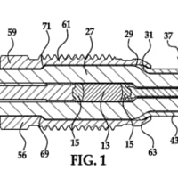
Referring back to FIG. 1A, the laser beams 102 generated by VCSEL array 110 are demagnified and focused on the backside of a photocathode 130 using a demagnifying light optics 120. Photons of laser beams 102 excite electrons in photocathode 130 above the vacuum level. Excited electrons that do not lose enough energy while scattering in photocathode 130 are emitted into vacuum as electron beams 103 and conventionally accelerated towards writing plane 101. A variety of photocathodes can be used with the invention including negative electron affinity (NEA) photocathodes, cesium-tellurium (CsTe) photocathodes, and silicon-cesium oxide nanoclusters. NEA photocathodes are commercially available from Intevac, Inc. of Santa Clara, Calif. and are described in U.S. Pat. No. 5,684,360 to Baum et al., incorporated herein by reference in its entirety. CsTe photocathodes require a VCSEL 112 with a relatively short wavelength (e.g., about 300 nm) while NEA photocathodes require a VCSEL 112 with a relatively long wavelength (e.g., about 700 nm). Electron beams 103 that are emitted from photocathode 130 are demagnified and scanned(スキャン)across writing plane 101 using a demagnifying and scanning electron optics 140.
FIG. 1B schematically shows further details of lithography system 100. Demagnifying light optics 120 (FIG. 1A) is shown in FIG. 1B as including(含むものとして図示)an optical field lens 121 and an optical demagnifying lens 122. Optical field lens 121 focuses the divergent laser beams from VCSEL array 110 onto the optical demagnifying lens 122, which in turn demagnifies the laser beams for striking(照射)the photosensitive backside of photocathode 130.
In FIG. 1B, demagnifying and scanning electron optics 140 (FIG. 1A) is shown as including an electron field lens 141, a beam limiting aperture 142, a demagnifying electron lens 143, and an objective lens 144. As is known in the art, an electron optics includes magnetic (e.g., coils, pole pieces, yokes) and electrostatic components for influencing an electron beam. Divergent electron beams that are emitted from photocathode 130 are focused onto a beam limiting aperture 142. Electron beams passing through(通過)beam limiting aperture 142 are demagnified by demagnifying electron lens 143 before being focused onto writing plane 101 using objective lens 144. The present invention can also be implemented using the light and electron optics/lenses disclosed in commonly-assigned U.S. Patent Application, "Compact Photoemission Source, Field And Objective Lens Arrangement For High Throughput Electron Beam Lithography," Ser. No. 09/272,086, filed on Mar. 18, 1999, incorporated herein by reference in its entirety.
While the invention is described using specific examples, the invention is not so limited(実施例に限定されない)and may be practiced using alternative techniques which are readily apparent to one of ordinary skill in the art reading this disclosure(本開示を読めば). The scope of the present invention is set forth in the following claims.
最新の画像[もっと見る]
-
 流入出口
5日前
流入出口
5日前
-
 弁室
1週間前
弁室
1週間前
-
 わたって重なる
2週間前
わたって重なる
2週間前
-
 絶縁碍子
2週間前
絶縁碍子
2週間前
-
 絶縁碍子
2週間前
絶縁碍子
2週間前
-
 絶縁碍子
2週間前
絶縁碍子
2週間前
-
 絶縁碍子
2週間前
絶縁碍子
2週間前
-
 CDプレーヤー修理:ア~ムカミン!
2週間前
CDプレーヤー修理:ア~ムカミン!
2週間前
-
 CDプレーヤー修理:ア~ムカミン!
2週間前
CDプレーヤー修理:ア~ムカミン!
2週間前
-
 CDプレーヤー修理:ア~ムカミン!
2週間前
CDプレーヤー修理:ア~ムカミン!
2週間前


