US2015287425
[0036] FIG. 7(a) shows the absorption cross-section of spherical plasmonic nanoparticles with a 15 nm radius.
図7(a)は、半径15nmの球状プラズモニックナノ粒子の吸収断面積を示す。
Dielectric permittivities retrieved from thin films of Au and TiN, grown at 400° C. and 800° C., are used in the calculation for accurate results.
400℃および800℃でAuおよびTiNの薄膜を成長させて、誘電率を測定し、吸収断面積を正確に算出した。
The results show that TiN provides better absorption efficiencies when compared to Au.
その結果、Auと比較してTiNは優れた吸収効率を有することが示された。
Due to the non-stoichiometric nature of TiN, it is also possible to obtain particles with different resonance strengths and spectral positions.
TiNは不定比化合物であることから、共鳴強度やスペクトル位置の異なる粒子を得ることも可能である。
WO2014065949
[0008] In addition to being flat, the substrates must also be smooth and free of mechanical damage on the surface.
平坦であることに加えて、基板は滑らかで、表面上に機械的損傷のないものでなければならない。
This requirement is mandatory, as part of the device fabrication process the substrate will be placed into a chemical vapor deposition epitaxy process, which is used to grow crystalline thin films.
この要求は、結晶性薄膜を成長させるのに使用する化学気相成長エピタキシプロセス中に基板が置かれるデバイス製造プロセスの一部として、必須である。
As the thin film grows, it replicates the crystal structure presented on the substrate's surface.
薄膜が成長するにつれて、この薄膜は基板の表面上に生じる結晶構造を複製する。
Consequently, excessive roughness and mechanical damage on the substrate's surface would result in poor film quality.
結果として、基板表面の過度な粗さ及び機械的損傷により、膜質の劣化をもたらすであろう。
WO2010096261
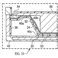
[0038] At block 188 (FIG. 4), the trench dielectric layers 123, 163, and 167 may be formed.
ブロック188(図4)では、トレンチ誘電体層123、163および167を形成してよい。
This action may comprise growing a thin oxide layer on the trench sidewalls at a high temperature of HOO0C or more in a dry oxygen environment (no water vapor) that is diluted with an inert gas.
この動作は、不活性ガスで希釈されたドライ酸素環境(水蒸気を含まない)で、1100℃以上の高温でトレンチの側壁上に酸化薄膜を成長させるステップを含んでよい。
The oxide layer, which is also referred to herein as the "shield oxide layer," may be grown to a thickness in the range of about 400 Angstroms to 600 Angstroms, with a thickness of about 500 Angstroms being preferred.
本願で「シールド酸化膜」ともいう酸化膜を、約400オングストロームから600オングストロームの範囲の厚さに成長させてよいが、約500オングストロームの厚さが好ましい。
Since the mesa tops are exposed during the growth process, the shield oxide layer is also formed over the mesa tops.
成長プロセス中、メサのトップが露出されるので、シールド酸化膜は、メサのトップにも形成される。
In one typical implementation, the growth temperature is in the range of 11250C to 12000C,
一般的な実現例では、成長温度は、1125℃から1200℃の範囲であるが、
with a value of about 11750C (±10°C) being preferred, and the environment comprises 50% oxygen and 50% argon (e.g., flow rate of each gas of 10 liters per minute).
約1175℃(±10℃)の値が好ましく、環境は、50%の酸素と50%のアルゴン(例えば、毎分10リットルの各ガスの流量)からなる。
The combined use of the high growth temperature and diluted dry oxygen environment to grow the shield oxide layer is unusual in the power semiconductor art,
電力用半導体技術では、シールド酸化膜を成長させるために高い成長温度と希釈されたドライ酸素環境とを組み合わせて使用することは普通のことではないが、
but the inventors have found that this combination provides fewer pinhole defects in the layer leading to improved gate oxide quality, higher values of QjxJ (charge to breakdown), and a better thickness uniformity.
本発明者たちは、このように組み合わせると、膜内のピンホール欠陥がほとんどなくなり、これによってゲート酸化膜の質が改善され、Qbd(電荷対ブレークダウン)の値がより高くなり、厚さの均一性がより良好となることを発見した。
The oxygen may be diluted such that it composes 10% to 75% by volume of the gaseous growth environment, and more preferably 25% to 60% by volume of the gaseous growth environment.
酸素は、気相成長環境の10容積%から75容積%、より好ましくは25容積%から60容積%を構成するように酸素を希釈してよい。
By the end of this processing, the trenches may have widths of about 0.5 microns and depths of about 1.1 microns, and the mesas may have widths of about 0.3 microns for a typical implementation of device 100.
このプロセスの終りまでに、デバイス100の一般的な実現例として、トレンチは約0.5ミクロンの幅および約1.1ミクロンの深さを有し、メサは約0.3ミクロンの幅を有し得る。