


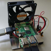
ルネサス製のRX210マイコンのSCI0を使用したシリアル通信プログラムのサンプルです。
リングバッファと割り込みを使用しています。
change_oscillation_PLL()関数
リングバッファと割り込みを使用しています。
- /*
- * interrupt_handlers.c のSCI0関連の割り込みをコメントアウトすること
- * // SCI0 ERI0
- * //void Excep_SCI0_ERI0(void){ }
- *
- * // SCI0 RXI0
- * //void Excep_SCI0_RXI0(void){ }
- *
- * // SCI0 TXI0
- * //void Excep_SCI0_TXI0(void){ }
- *
- * // SCI0 TEI0
- * //void Excep_SCI0_TEI0(void){ }
- *
- */
- #include "iodefine.h"
- #include <stdio.h>
- #include <machine.h>
- #include "vect.h"
- #define PCLK 25 //PクロックMHz
- #define TX_ACTIVE 1 //送信動作中
- #define TX_INACTIVE 0 //送信停止中
- #define TX_RING_BUFF_SIZE 32 //リングバッファのサイズ
- #define RX_RING_BUFF_SIZE 32 //リングバッファのサイズ
- //リングバッファ
- unsigned char rx_buff[RX_RING_BUFF_SIZE]; //受信用
- unsigned char tx_buff[TX_RING_BUFF_SIZE]; //送信用
- //データポインタ
- volatile int ptr_rx_top,ptr_rx_bottom;
- volatile int ptr_tx_top,ptr_tx_bottom;
- //送信フラグ データ送信中かどうか
- volatile int tx_flag = TX_INACTIVE;
- /*
- * SCI0初期化
- * 57600bps: 8bit: stop bit 1: Parity none
- * PCLK 25MHz
- */
- void SCI_Init (void)
- {
- /* ---- SCI interrupt request is disabled ---- */
- IR(SCI0,ERI0) = 0;
- IR(SCI0,RXI0) = 0;
- IR(SCI0,TXI0) = 0;
- IR(SCI0,TEI0) = 0;
- /* ---- Initialization of SCI ---- */
- /* PRCR - Protect Register
- b15:b8 PRKEY - PRC Key Code - A5h (The write value should be A5h to permission writing PRCi bit)
- b7:b4 Reserved - The write value should be 0.
- b1 PRC1 - Protect Bit 1 - Write enabled */
- SYSTEM.PRCR.WORD = 0xA502;
- /* The module stop state of SCIn is canceled */
- MSTP(SCI0) = 0;
- /* Enable write protection */
- SYSTEM.PRCR.WORD = 0xA500;
- /* SCR - Serial Control Register
- b7 TIE - Transmit Interrupt Enable - A TXI interrupt request is disabled
- b6 RIE - Receive Interrupt Enable - RXI and ERI interrupt requests are disabled
- b5 TE - Transmit Enable - Serial transmission is disabled
- b4 RE - Receive Enable - Serial reception is disabled
- b2 TEIE - Transmit End Interrupt Enable - A TEI interrupt request is disabled */
- SCI0.SCR.BYTE = 0x00;
- while (0x00 != (SCI0.SCR.BYTE & 0xF0))
- {
- /* Confirm that bit is actually 0 */
- }
- /* ---- Set the I/O port functions ---- */
- /* Set port output data - High level */
- PORT2.PODR.BIT.B0 = 1;
- /* Set port direction - TXDn is output port, RXDn is input port */
- PORT2.PDR.BIT.B0 = 1;
- PORT2.PDR.BIT.B1 = 0;
- /* Set port mode - Use pin as general I/O port */
- PORT2.PMR.BIT.B1 = 0;
- PORT2.PMR.BIT.B0 = 0;
- /* PWPR - Write-Protect Register
- b7 B0WI - PFSWE Bit Write Disable - Writing to the PFSWE bit is enabled
- b6 PFSWE - PFS Register Write Enable - Writing to the PFS register is enabled
- b5:b0 Reserved - These bits are read as 0. The write value should be 0. */
- MPC.PWPR.BIT.B0WI = 0;
- MPC.PWPR.BIT.PFSWE = 1;
- /* PFS - Pin Function Control Register
- b3:b0 PSEL - Pin Function Select - RXDn, TXDn */
- MPC.P20PFS.BYTE = 0x0A;
- MPC.P21PFS.BYTE = 0x0A;
- /* Enable write protection */
- MPC.PWPR.BIT.PFSWE = 0;
- MPC.PWPR.BIT.B0WI = 1;
- /* Use pin as I/O port for peripheral functions */
- PORT2.PMR.BIT.B1 = 1;
- PORT2.PMR.BIT.B0 = 1;
- /* ---- Initialization of SCI ---- */
- /* Select an On-chip baud rate generator to the clock source */
- SCI0.SCR.BIT.CKE = 0;
- /* SMR - Serial Mode Register
- b7 CM - Communications Mode - Asynchronous mode
- b6 CHR - Character Length - Selects 8 bits as the data length
- b5 PE - Parity Enable - When transmitting : Parity bit addition is not performed
- When receiving : Parity bit checking is not performed
- b3 STOP - Stop Bit Length - 1 stop bits
- b2 MP - Multi-Processor Mode - Multi-processor communications function is disabled
- b1:b0 CKS - Clock Select - PCLK clock (n = 0) */
- SCI0.SMR.BYTE = 0x00;
- /* SCMR - Smart Card Mode Register
- b6:b4 Reserved - The write value should be 1.
- b3 SDIR - Transmitted/Received Data Transfer Direction - Transfer with LSB-first
- b2 SINV - Transmitted/Received Data Invert - TDR contents are transmitted as they are.
- Receive data is stored as it is in RDR.
- b1 Reserved - The write value should be 1.
- b0 SMIF - Smart Card Interface Mode Select - Serial communications interface mode */
- SCI0.SCMR.BYTE = 0xF2;
- /* SEMR - Serial Extended Mode Register
- b7:b6 Reserved - The write value should be 0.
- b5 NFEN - Digital Noise Filter Function Enable - Noise cancellation function
- for the RXDn input signal is disabled.
- b4 ABCS - Asynchronous Mode Base Clock Select - Selects 16 base clock cycles for 1-bit period
- b3:b1 Reserved - The write value should be 0. */
- SCI0.SEMR.BYTE = 0x00;
- /* BRR - Bit Rate Register
- Bit Rate: (25MHz/(64*2^(-1)*57600bps))-1=12.56 */
- SCI0.BRR = 13; /* 57600bps */
- //SCI0.BRR = 40; /* 19200bps */
- /* ---- Initialization of SCI interrupt ---- */
- /* SCI interrupt priority level is 1 */
- IPR(SCI0, ) = 1;
- /* Interrupt request is cleared (Edge interrupt) */
- IR(SCI0,RXI0) = 0;
- IR(SCI0,TXI0) = 0;
- /* 割り込みの許可 */
- IEN(SCI0, RXI0) = 1;
- IEN(SCI0, ERI0) = 1;
- IEN(SCI0, TXI0) = 1;
- IEN(SCI0, TEI0) = 1;
- /* リングバッファの初期化 */
- ptr_rx_top = ptr_rx_bottom = 0;
- ptr_tx_top = ptr_tx_bottom = 0;
- /* 送受信許可 */
- SCI0.SCR.BIT.RIE = 1; //受信割込み
- SCI0.SCR.BIT.TIE = 1; //送信割込み
- SCI0.SCR.BIT.RE = 1; //受信動作開始
- SCI0.SCR.BIT.TE = 0;
- }
- /*
- * 受信エラー割り込み
- */
- /* SSR - Serial Status Register
- b7:b6 Reserved - The read value is undefined. The write value should be 1.
- b5 ORER - Overrun Error Flag - An overrun error has occurred
- b4 FER - Framing Error Flag - A framing error has occurred
- b3 PER - Parity Error Flag - A parity error has occurred */
- #define SSR_ERROR_FLAGS (0x38)
- void Excep_SCI0_ERI0(void)
- {
- volatile char c;
- c = SCI0.RDR; //ダミーリード
- SCI0.SSR.BYTE = (SCI0.SSR.BYTE & ~SSR_ERROR_FLAGS) | 0xC0; //エラーフラグクリア
- }
- /*
- * 受信バッファフル割込み
- */
- void Excep_SCI0_RXI0(void)
- {
- /* Read data */
- rx_buff[ptr_rx_top] = SCI0.RDR;
- ptr_rx_top++;
- ptr_rx_top = ptr_rx_top % RX_RING_BUFF_SIZE;
- }
- /*
- * 送信バッファエンプティ割込み
- */
- void Excep_SCI0_TXI0(void)
- {
- if( ptr_tx_bottom == ptr_tx_top ) { //送信するデータがない
- SCI0.SCR.BIT.TEIE = 1; //送信終了割り込みの発生を待つ
- } else {
- /* Write the character out */
- SCI0.TDR = tx_buff[ptr_tx_bottom];
- ptr_tx_bottom++;
- ptr_tx_bottom = ptr_tx_bottom % TX_RING_BUFF_SIZE;
- }
- }
- /*
- * 送信終了割り込み
- */
- void Excep_SCI0_TEI0 (void)
- {
- SCI0.SCR.BIT.TE = 0; //送信停止
- IR(SCI0,TXI0) = 0; //割り込みフラグクリア
- SCI0.SCR.BIT.TEIE = 0; //送信完了割込み停止
- tx_flag = TX_INACTIVE; //送信回路フラグを停止に
- }
- /*
- * データの送信
- */
- void SCI_put(unsigned char output_char)
- {
- int tmp;
- tmp = ptr_tx_top + 1;
- tmp = tmp % TX_RING_BUFF_SIZE;
- while(tmp == ptr_tx_bottom) ; //バッファに空きができるまで待つ
- tx_buff[ptr_tx_top] = output_char;
- ptr_tx_top++;
- ptr_tx_top = ptr_tx_top % TX_RING_BUFF_SIZE;
- if(tx_flag == TX_INACTIVE) {
- tx_flag = TX_ACTIVE; //送信回路フラグを動作に
- SCI0.SCR.BIT.TE = 1; //送信割込み許可
- SCI0.SCR.BIT.TEIE = 0; //送信完了割込み停止
- }
- }
- void charput(unsigned char c)
- {
- //while(IR(SCI0,TXI0)==0) ;
- if(c=='\r' || c=='\n') {
- SCI_put('\r');
- SCI_put('\n');
- } else {
- SCI_put(c);
- }
- }
- /* データの受信 バッファに受信したデータがなければ受信するまで待つ */
- unsigned int SCI_get(void)
- {
- unsigned char c;
- while(ptr_rx_bottom == ptr_rx_top); //データを受信するまで待つ
- c = rx_buff[ptr_rx_bottom];
- ptr_rx_bottom++;
- ptr_rx_bottom = ptr_rx_bottom % RX_RING_BUFF_SIZE;
- return c;
- }
- unsigned int charget(void)
- {
- return SCI_get();
- }
- /*
- * 文字列の出力
- */
- void printString(char *s)
- {
- while( *s != 0 ) {
- charput(*s);
- s++;
- }
- }
- /*
- * printf関数で使用
- */
- int _write(int file,char *ptr,int len)
- {
- int i;
- for(i=0;i<len;i++) {
- charput(ptr[i]);
- }
- return len;
- }
- /*
- * scanf関数で使用
- */
- int _read (int file, char *ptr, int len)
- {
- *ptr = charget();
- return 1;
- }
- void main(void)
- {
- char buf;
- change_oscillation_PLL(); //クロックソースPLL
- SCI_Init ();
- setpsw_i(); // 割込み許可 clrpsw_i()割込み禁止
- printString("RS232C test program\n");
- printString("use SCI0123\n");
- while(1) {
- buf = charget();
- _write(0,&buf,1);
- }
- }
change_oscillation_PLL()関数
/*
 *  動作クロックをPLLで50MHzに設定
*/
void change_oscillation_PLL(void)
{
	unsigned int i;

	/* ---- Enable write protection ---- */
    /* PRCR - Protect Register
    b15:b8  PRKEY - PRC Key Code - A5h
                  (The write value should be A5h to permission writing PRCi bit)
    b7:b4   Reserved - The write value should be 0.
    b3      PRC3 - Protect Bit 3 - Write disabled
    b2      PRC2 - Protect Bit 2 - Write enabled
    b1      PRC1 - Protect Bit 1 - Write enabled
    b0      PRC0 - Protect Bit 0 - Write enabled */
    SYSTEM.PRCR.WORD = 0xA507;

    /* ---- Set the VRCR register ---- */
    SYSTEM.VRCR = 0x00;

    /* ----  Set the main clock oscillator drive capability ---- */
    /* MOFCR - Main Clock Oscillator Forced Oscillation Control Register
    b7       Reserved - The write value should be 0.
    b6       MOSEL    - Main Clock Oscillator Switch - Resonator
    b5:b4    MODRV2   - Main Clock Oscillator Drive Capability Switch 2
                      - 16 MHz to 20 MHz
    b3:b1    MODRV    - Main Clock Oscillator Drive Capability Switch
                      - 16 MHz to 20 MHz non-lead type ceramic resonator
    b0       Reserved - The write value should be 0. */
    SYSTEM.MOFCR.BYTE = (0x30);	/* Drive capability : 20 MHz crystal resonator */

    /* ---- Set wait time until the main clock oscillator stabilizes ---- */
    /* MOSCWTCR - Main Clock Oscillator Wait Control Register
    b7:b5    Reserved - The write value should be 0.
    b4:b0    MSTS     - Main Clock Oscillator Waiting Time
                      - Wait time is 131072 cycles (approx. 6.55 ms). */
    SYSTEM.MOSCWTCR.BYTE = (0x0D);	/* Wait control register : 131072 cycles (approx. 6.55 ms) */

    /* ---- Operate the main clock oscillator ---- */
    /* MOSCCR   - Main Clock Oscillator Control Register
    b7:b1    Reserved - The write value should be 0.
    b0       MOSTP    - Main Clock Oscillator Stop - Main clock oscillator is operating. */
    SYSTEM.MOSCCR.BYTE = 0x00;

    while (0x00 != SYSTEM.MOSCCR.BYTE)
    {
        /* Confirm that the written value can be read correctly. */
    }


    /* ---- Wait processing for the clock oscillation stabilization ---- */
    for(i=0;i<100;i++) nop();

    /* ---- Set the PLL division ratio and multiplication factor ---- */
    /* PLLCR - PLL Control Register
    b15:b13  Reserved - The write value should be 0.
    b12:b8   STC      - Frequency Multiplication Factor Select
                      - Frequency multiplication factor is multiply-by-10.
    b7:b2    Reserved - The write value should be 0.
    b1:b0    PLIDIV   - PLL Input Frequency Division Ratio Select
                      - PLL input division ratio is divide-by-2. */
    SYSTEM.PLLCR.WORD = (0x0901);	/* Division ratio and multiplication factor : divide-by-2, multiply-by-10 */

    /* ---- Set wait time until the PLL clock oscillator stabilizes ---- */
    /* PLLWTCR - PLL Wait Control Register
    b7:b5    Reserved - The write value should be 0.
    b4:b0    PSTS     - PLL Waiting Time
                      - Wait time is 65536 cycles (approx. 655.36 us). */
    SYSTEM.PLLWTCR.BYTE = (0x09);	/* Wait control register : 65536 cycles (approx. 655.36 us) */

    /* ---- Operate the PLL clock oscillator ---- */
    /* PLLCR2 - PLL Control Register 2
    b7:b1    Reserved - The write value should be 0.
    b0       PLLEN    - PLL Stop Control - PLL is operating. */
    SYSTEM.PLLCR2.BYTE = 0x00;

    /* ---- Wait processing for the clock oscillation stabilization ---- */
    for(i=0;i<100;i++) nop();

    /* ---- Set the operating power control mode ---- */
    /* OPCCR - Operating Power Control Register
    b7:b5   Reserved - The write value should be 0.
    b4      OPCMTSF  - Operating Power Control Mode Transition Status Flag
    b3      Reserved - The write value should be 0.
    b2:b0   OPCM     - Operating Power Control Mode Select - High-speed operating mode */
    SYSTEM.OPCCR.BYTE = (0x00);          /* High-speed operating mode */

    while (0 != SYSTEM.OPCCR.BIT.OPCMTSF)
    {
        /* Confirm that the operation power control mode transition completed. */
    }

    /* ---- Set the internal clock division ratio ---- */
    /* SCKCR - System Clock Control Register
    b31:b28 FCK      - FlashIF Clock(FCLK) Select - divide-by-4
    b27:b24 ICK      - System Clock (ICLK) Select - divide-by-2
    b23     PSTOP1   - BCLK Pin Output Control    - disabled. (Fixed high)
    b22:b20 Reserved - The write value should be 0.
    b19:b16 BCK      - External Bus Clock (BCLK) Select - divide-by-4
    b15:b12 Reserved - The write value should be 0001b.
    b10:b8  PCLKB    - Peripheral Module Clock B(PCLKB) Select - divide-by-4
    b7:b4   Reserved - The write value should be 0001b.
    b3:b0   PCLKD    - Peripheral Module Clock D(PCLKD) Select - divide-by-2 */
    SYSTEM.SCKCR.LONG = 0x21821211;	/* ICLK,PCLKD: divide-by-2 PCLKB,BCLK,FCLK: divide-by-4 */

    while (0x21821211 != SYSTEM.SCKCR.LONG)
    {
         /* Confirm that the written value can be read correctly. */
    }

    /* ---- Set the BCLK pin output ---- */
    /* BCKCR - External Bus Clock Control Register
    b7:b1   Reserved - The write value should be 0.
    b0      BCLKDIV  - BCLK Pin Output Select - divide-by-2 */
    SYSTEM.BCKCR.BYTE = 0x01;

    while (0x01 != SYSTEM.BCKCR.BYTE)
    {
        /* Confirm that the written value can be read correctly. */
    }

    /* ---- Set the internal clock source ---- */
    /* SCKCR3 - System Clock Control Register 3
    b15:b11 Reserved - The write value should be 0.
    b10:b8  CKSEL    - Clock Source Select - PLL circuit is selected.
    b7:b1   Reserved - The write value should be 0. */
    SYSTEM.SCKCR3.WORD = (0x0400);	/* PLL */

    while ((0x0400) != SYSTEM.SCKCR3.WORD)
    {
        /* Confirm that the written value can be read correctly. */
    }

    /* ---- Disable write protection ---- */
    /* PRCR - Protect Register
    b15:b8 PRKEY - PRC Key Code - A5h
                  (The write value should be A5h to permission writing PRCi bit)
    b2     PRC2 - Protect Bit 2 - Write disabled
    b1     PRC1 - Protect Bit 1 - Write disabled
    b0     PRC0 - Protect Bit 0 - Write disabled */
    SYSTEM.PRCR.WORD = 0xA500;

}
</pre>


RX210でRS232Cを使う その2で
#include "iodefine.h"
/* ---- Set the VRCR register ---- */
SYSTEM.VRCR = 0x00; ←ここでエラーが出ます
VRCRが無いというエラーです
どう定義したらいいのでしょうか?
CPUは RX-210です
簡単なことですみません
メールは tabu512@yahoo.co.jp です
RX210のシリアル通信サンプルプログラムを探してここにたどり着きました。
ここのサンプルのおかげで簡単に動かすことができました。ありがとうございました。