


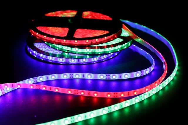
LED is called the fourth generation light source, with energy-saving, environmental protection, safety, long life (up to 100,000 hours), low power consumption, low heat, high brightness, waterproof, miniature, shock-proof, easy dimming, beam concentration, easy maintenance and other characteristics. It meets the requirements of energy saving, green and efficient era. It can be widely used in various fields such as indication, display, decoration, backlight, general lighting and so on.
LED is essentially a PN junction, through the P region hole and N region electron compound to produce photons, electrical energy directly converted to light energy, is a cold light source. But the traditional incandescent lamp is the electric heating filament, the electric energy transforms into the thermal energy, then transforms from the thermal energy to the light energy. So the efficiency of LED is much higher than that of incandescent lamps.
The LED industry chain includes upstream epitaxial manufacturing, midstream chip preparation, electrode fabrication, cutting and test sorting, downstream product packaging. Epitaxial films are in the upper reaches of the industry, including three major fields: raw materials, substrate materials and equipment. Epitaxial film growth is the highest technology content of lighting industry, and has the greatest impact on the final product quality and cost control.
Most of the LED epitaxial wafers are III-V compound semiconductor single crystals, such as gallium arsenide, aluminum nitride, gallium nitride, gallium phosphide, gallium arsenide phosphide, phosphorus compounds (blue-green light), aluminum calcium indium nitrogen (quaternary LED, red-yellow light), and other single crystals. The raw materials used to prepare these single crystals include indium, high-purity gallium, organometallic gallium, aluminum, etc. Epitaxial growth depends mainly on growth technology and equipment. The main method of fabricating epitaxial wafers is metal organic chemical vapor deposition (MOCVD), which is very difficult to fabricate.
The substrate material is the basis of LED illumination and epitaxial growth. Different substrate materials need different epitaxial growth technology, which affects chip processing and device packaging. Therefore, the technical route of substrate materials will affect the technical route of the entire industry, which is the key of each technical link. At present, Al2O3 (sapphire), SiC, Si, GaN, GaAs, ZnO, ZnSe and so on can be used as substrate materials, but the most widely used commercial Al2O3 (sapphire) and SiC.
Stanford Advanced Materials provides high-purity organometallic compounds for epilayers, substrate materials, photoresist for chip fabrication, high-temperature molybdenum, tungsten drying pots and furnace assemblies and fixtures in MOCVD processes (these high-temperature materials have high thermal conductivity and electrical conductivity, up to 2000 degrees Celsius). It has the characteristics of low thermal expansion coefficient, high strength and stability, and epoxy resin for chip packaging.


※コメント投稿者のブログIDはブログ作成者のみに通知されます