非常に素晴らしい先端材料

金属材料、コーティング材料、セラミック材料などを含むがこれらに限定されない驚くべき高級材料について

Advanced Indium Tin Oxide Target Embedded in Apple Iphone

2019年11月12日 | sputter target
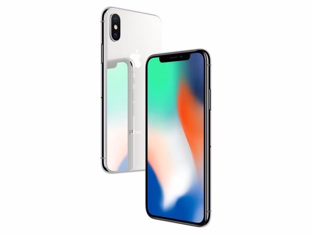
With the recent launch of the new generation iPhone X, iphone has once again become the focus of the market. Many people do not know that in the production of iphone display, the core material for the LCD screen to achieve touch is indium tin oxide (ITO) target.

Indium tin oxide (ITO) is a ternary composition of indium, tin and oxygen in varying proportions. Depending on the oxygen content, it can either be described as a ceramic or alloy. Indium tin oxide is typically encountered as an oxygen-saturated composition with a formulation of 74% In, 18% O2, and 8% Sn by weight. Oxygen-saturated compositions are so typical, that unsaturated composition is termed oxygen-deficient ITO. It is transparent and colorless in thin layers, while in bulk form it is yellowish to grey. In the infrared region of the spectrum, it acts as a metal-like mirror. Indium tin oxide is obtained by mixing two oxides of indium trioxide and tin dioxide in a certain ratio, and tin dioxide generally accounts for 10% of the total weight.

Indium tin oxide conductive film is referred to as the "nerve" of the touch LCD screen. In the production process of the liquid crystal panel, the indium tin oxide target is placed in a vacuum environment, and is bombarded with an electron beam, and the generated particles are dispersed on the screen substrate to form a transparent indium tin oxide conductive film. Because of the existence of these conductive films, the liquid crystal display can sense the static electricity of the fingers and realize touch control. When the thickness of the film does not exceed a few hundred nanometers (one nanometer is one-billionth of a meter), 80% or more of visible light can be transmitted, so it does not greatly affect the transparency of glass or plastic. At the same time, this layer of indium tin oxide film has a strong electrical conductivity, and the resistivity can be as low as one ten-thousandth of an ohm•meter. The perfect combination of light transmission and electrical conductivity makes indium tin oxide the only choice for producing touch screens.

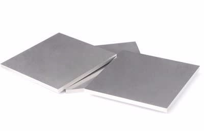
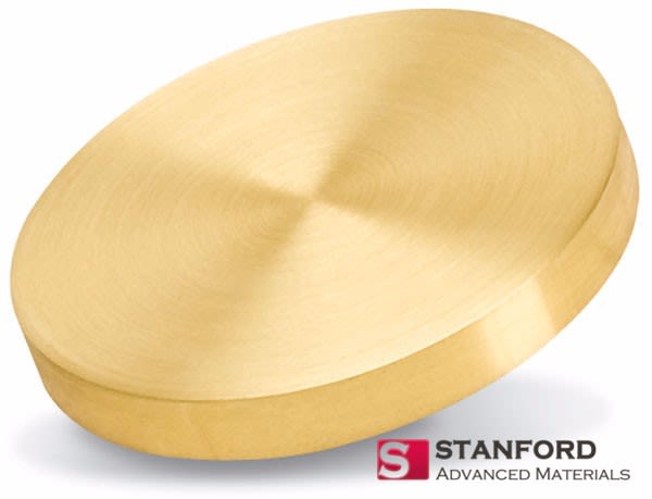
Sputtering targets are not only the core materials in the field of flat panel displays, but also widely used in solar cells, electrochromic functional films, infrared remote sensing detectors and other fields. At present, the innovative target atmospheric pressure sintering process solves the problem of high input cost of high-pressure sintering, poor technical stability, and difficulty in large-scale production. In addition, the major sputtering target companies have achieved large-scale, high-density and low-resistivity products, and are committed to improving core performance indicators such as relative density, purity and resistivity.
  
Nowadays, ITO targets are setting off a new round of enthusiasm, and ITO targets are being further expanded in the fields of high-end thin film transistor liquid crystal displays. For more information, please visit https://www.sputtertargets.net/.

Factors Affecting the Quality and Function of Tantalum Film

2019年08月07日 | sputter target
There are three factors that affect the quality and function of the tantalum film: 1) the nature and structure of the material to be deposited (ie, the metal tantalum), 2) the quality and performance of the source material (ie, the tantalum target), and 3) the inherent performance and layout of the deposition system and its associated peripherals.

The nature and structure of the material to be deposited cannot be changed. The only thing you can do is to change another material, such as aluminum, molybdenum, or else.

Tantalum is dense, ductile, very hard, easily fabricated, and highly conductive of heat and electricity, which is a good coating material. So you don't need to worry about its inherent nature will have bad influence on the deposited film. Also, this article does not discuss the first factor but focuses on the latter two factors.

The sputtering industry has high requirements for source materials. The tantalum target used for sputter coating generally has a purity between 2N and 5N. While for special industries, such as the electronics industry, the purity requirement of the tantalum target is generally before 4N-6N.


In addition to purity, density is also an important measure of the target quality. The density of the target material not only affects the sputtering rate, but also affects the electrical and optical properties of the film. In general, the higher the density of the target material, the better the performance of the film. Additionally, increasing the density and strength of the target material allows the target material to better withstand thermal stresses during sputtering.

Another measure of the quality of the deposition source is the grain size. For the same target material, the sputtering rate of the target having a small grain size is faster than the sputtering rate of the target having a large grain size; the thickness distribution of the target sputtering film having a small grain size difference is more uniform. In order to obtain qualified bismuth targets, we recommend purchasing from Stanford Advanced Materials, a global sputtering target supplier.

After talking about the source material, let's take a look at the deposition system. Undoubtedly, if a sputtering system with poor sealing properties, structural disorder, and old equipment is used for coating, even if the source material is good, a satisfactory film cannot be deposited. Therefore, a well-designed, well-equipped sputtering system is essential. It is still recommended that you purchase a sputter machine from a trusted manufacturer and have regular maintenance to ensure that the system is operating properly.

For more information, please visit https://www.sputtertargets.net/sputtering-target.html.

7 facts about semiconductor silicon wafer

2019年04月11日 | sputter target
1. Semiconductor, as it literally seems to be, is a solid substance whose conductivity is between insulator and most metals, either due to the addition of an impurity or because of temperature effects. In other words, the conductivity of the semiconductor can be controlled by adding impurities as a specific amount of other materials to the semiconductor.

2.Most semiconductor wafers are made of silicon, which is the second-most abundant element in the Earth's crust (about 28% by mass) after oxygen and the eighth-most common element in the entire universe by mass. In addition to silicon, semiconductors also use other materials, including germanium, gallium arsenide, germanium, indium phosphide, sapphire and quartz.

3. Semiconductor wafers are available in a spread of diameters. The first semiconductor wafer made inside the US in 1960 was just 1 inch in diameter. Today, standard semiconductor wafers go up to 12 inches to 18 inches.

4. Sputtering target is an importanced material for semiconductor coating. Usually, semiconductors have the highest technical requirements and purity requirements, which are significantly higher than other applications such as flat panel displays and solar cells. Thus, the price of high quality sputtering target used for semiconductor is also the most expensive.

5. Water is the key component of manufacturing Silicon wafers. It is a compound that basically is a general solvent for all substances, silicon included. A large production facility uses up to 4.8 million of gallons of water everyday to supply Silicon wafers for manufacturing needs and supply.

6. The thickness of semiconductor wafers vary greatly. The thickness of wafer is always determined by the mechanical strength of any material used to make it. Regardless of what the semiconductor is made of, the wafer must be thick enough to support its own weight so that it does not break during processing.

7. Contamination is inevitable during the manufacture and transportation of semiconductors. Appropriate storage conditions must be in place to prevent contamination and/or degradation after shipment. Semiconductor wafers that are not vacuum sealed must be placed in a Nitrogen (N2) cabinet at a flow rate of 2 to 6 SCFH (Standard Cubic Feet per Hour).

Please visit https://www.sputtertargets.net/ for more information.

What is PVD Gold Sputtering?

2019年01月29日 | sputter target
Gold is a popular precious metal that has been used for centuries as currency, hedging and jewelry for its noble and beautiful gold color. People love the gold color. But at the same time, the price of gold is high because of its scarcity. Gold coating is a good solution to this problem.


Gold sputtering is a thin film deposition process in which gold or gold alloy is bombarded with high energy ions in a vacuum chamber, causing gold atoms or molecules to be "sputtered" into the vapor and condensed on the substrate to be coated. Sputtering is a method of PVD process, the other two of which are thermal evaporation deposition and electron beam vapor deposition.
These two methods can also be used to coat gold film: in thermal evaporation deposition, the solid gold evaporates in a low-pressure environment with resistive heating elements; and in electron beam vapor deposition, the gold is heated by an electron beam, and then condensed on the substrate to be coated. Since gold coating just deposits a thin film on the subject, it demands a small quantity of pure gold material, so its price is cheaper.


Apart from PVD gold sputtering, there are other ways for gold coatings such as gold plating and gold filling.
Gold plating is a method which deposits a thin layer of gold on the surface of another metal by chemical or electrochemical plating. The advantages of gold plating are inexpensive and easy. However, the film obtained by this method is relatively soft and less durable. What’s worse, its chemical process would cause pollution that is bad for the environment.
Gold Filling is the mechanical bonding of gold to metal under high temperature and pressure. It produces a thicker coating than PVD gold sputtering and gold plating, and thus it is usually more expensive.


The constant contact of skin or clothing may abrade the coatings, especially in watch and jewelry industry. Thus, PVD gold sputtering is preferred in these two industries because the coatings it produces are harder and more durable than that of electrolytic gold plating or gold filling. Compared to other types of gold coatings, the main advantages of PVD gold sputtering coating are their durability, retention of gloss, corrosion resistance and abrasion resistance in contact with the skin, thus extending the life of jewelry. PVD gold sputtering not only provides the exact color and brightness which evokes the general feeling of love and attraction with jewelry, but also has the advantage of being more environmentally friendly and durable than gold plating or gold filling for producing a gold coating.

Founded in 1994, Stanford Advanced Materials(SAM) is a global sputtering targets manufacturer which supplies high-quality and consistent products to meet our customers’ R&D and production needs. Please visit https://www.sputtertargets.net/ for more information.

Things You Should Know About Target Bonding

2018年11月27日 | sputter target
 Common Materials for Bonding Sputtering Targets

1. Indium bonding: indium is the commonest and most cost-effective bonding material for brittle sputtering targets. The melting point of Indium is as high as 156.6°C, and thus the operating temperature should not exceed 156 ℃.

2. Silver filled Epoxy: Silver filled epoxy has a higher melting point than that of indium. Thus Silver filled epoxy will resist higher temperature. However, its high hardness might result in the breaking of targets. additionally, the price of Silver is much higher.

 Backing Plate Materials

1. Oxygen Free Copper: Oxygen Free Copper (OFHC) is the commonest backing plate material. It has excellent electrical and thermal conductivity properties and is easy to machine.

2. Molybdenum Plate: Mo plates are usually used when copper plates aren't appropriate for the application. For instance, once a high-temperature bond is needed, Copper might oxidize or warp. At this time, the molybdenum plate is applied.


 Cleaning

1. Metal Targets: Metal targets are often polished by alcohol and asepsis materials. Pre-sputtering is suggested at the start of the method.
2. Nonmetal Targets: Nonmetal targets are often polished by non-impregnated scotch bright and asepsis materials. Pre-sputtering is suggested at the start of the method.

 Storage
1. It is not recommended to store the sputtering targets in a vacuum.
2. Don’t touch the targets with ungloved hands. Always handle targets using protective gloves.

Please visit our website for more information.